Making method for multi-crystal TFT array of active driven organic EL display screen

A production method and luminescent technology, which are applied in the manufacture of circuits, electrical components, semiconductors/solid-state devices, etc., can solve problems such as difficulty, high cost, and complex process of polysilicon thin-film transistor arrays, and achieve the effect of simple process and feasible operation

Inactive Publication Date: 2008-02-13
JILIN UNIV
View PDF0 Cites 14 Cited by
  • Summary
  • Abstract
  • Description
  • Claims
  • Application Information

AI Technical Summary

Problems solved by technology

[0006] The process of preparing polysilicon thin film transistor arrays is complex and costly. Usually, the production of

Method used


Image

  • Making method for multi-crystal TFT array of active driven organic EL display screen
  • Making method for multi-crystal TFT array of active driven organic EL display screen
  • Making method for multi-crystal TFT array of active driven organic EL display screen

Examples


Example Embodiment

[0070] Example 1:

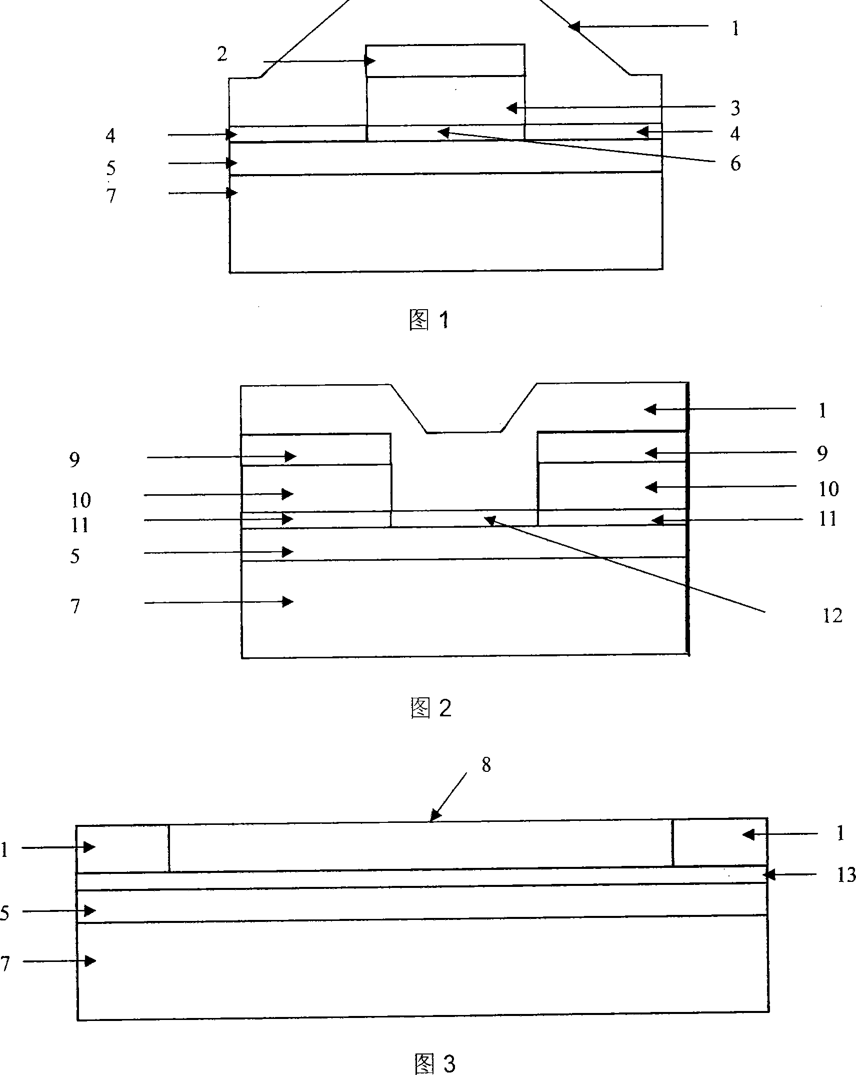
[0071] (1) On the annealed 100mm Corning 1737 glass substrate 7, ultrasonic cleaning with organic solvents such as toluene, acetone, ethanol, cleaning, drying with a nitrogen gun, PECVD method (TEOS, Tetra-Ethyl -Ortho-Silicate) decomposition, the substrate temperature is 350°C) deposition of 500nm low temperature silicon oxide (LTO: low temperature oxide) buffer layer 5 to block impurities in the glass;

[0072] (2) PECVD method deposits 60nm intrinsic amorphous silicon (a-Si) layer 14, substrate temperature 200℃, background vacuum 2×10 -4 pa, reaction chamber pressure 80pa, SiH 4 Flow rate 40sccm;

[0073] (3) PECVD method to deposit 60nm SiN x Insulation layer 15, using SiH 4 And NH 3 Mixed gas, substrate temperature 270℃, reaction chamber pressure 30Pa;

[0074] (4) Sputtering 30 induces the metal (Ni) layer 16, the substrate temperature is 130°C, and the background vacuum is 2×10 -4 Pa, the pressure of the reaction chamber during sputtering is 0.1 Pa; the...


PUM


Abstract

The invention belongs to flat panel display driving technique field and in particular relates to a method for manufacturing polysilicon TFT array of the active driving organic electroluminescent display panel. Firstly, a polysilicon film is manufactured and photoengraved to form a TFT area, a capacitance lower polar plate area, an anode area of the organic electroluminescent diode and a heavy doped polysilicon connection wire. A grid insulsting layer is manufactured and is photoengraved into pierced holes for connecting polysilicon with metal. The metal is then sputtered and photoengraved to form a metal grid and a metal connection wire. At the same time a doping window is opened in the capacitance lower polar plate doping area and then autoregistration is used to carry out the doping process and to carry out a heavy(BH3)P doping process on the source and drain electrode of TFT, polysilicon short stiring intereconnection area, and the areas needing doping in the capacitance lower polar plate. Finally, an insulating layer, a luminescent window, and an OLED luminescent layer are manufactured. The whole technique processes of method of the invention only need 4 photoengraving and reduce 2 photoengraving processes compared with the common Poly-Si TFT technique process, and has the good effects of having simple techniques.

Description

Technical field [0001] The invention belongs to the technical field of flat panel display driving, and in particular relates to a method for actively driving a polysilicon (Poly-Si) TFT array in an organic electroluminescent display (OLED). Background technique [0002] Organic electroluminescent displays (OLEDs) have become flat panel displays in recent years with their superior performance such as low power consumption, ultra-light and thin, bright colors, wide viewing angles, self-luminous, low cost, high brightness, flexibility, and ability to work normally under low temperature conditions. The focus of attention in the technical field. [0003] Organic light-emitting display screens can be divided into passive (Passive Matrix, PMOLED) and active (Active Matrix, AMOLED) according to their different driving methods. In addition to the light-emitting material itself, each pixel of the active drive display screen integrates multiple thin film transistors (TFT) on its substrate t...

Claims


Application Information

Patent Timeline
IPC IPC(8): H01L21/84
Inventor 张彤王丽杰刘雪强李传南刘式墉
Owner JILIN UNIV
Why Eureka
Try Eureka