MEMS Stacked Millimeter-Wave Antenna

A millimeter-wave antenna and electrical stacking technology, applied in the field of antennas, can solve the problems of low radiation efficiency, narrow bandwidth, and performance degradation of microstrip antennas

Active Publication Date: 2011-12-07
NO 55 INST CHINA ELECTRONIC SCI & TECHNOLOGYGROUP CO LTD
View PDF0 Cites 1 Cited by
  • Summary
  • Abstract
  • Description
  • Claims
  • Application Information

AI Technical Summary

Problems solved by technology

This requires the antenna to be fabricated on a high-permittivity dielectric substrate. However, compared with a low-permittivity dielectric substrate, a high-permittivity substrate is more likely to excite surface waves, and at the same time produces a larger dielectric Loss, the performance of the microstrip antenna is significantly reduced, the radiation efficiency is lower, the bandwidth is narrower, the radiation pattern is deteriorated, and unnecessary coupling is generated between the radiation elements in the array structure, etc.

Method used


Image

  • MEMS Stacked Millimeter-Wave Antenna
  • MEMS Stacked Millimeter-Wave Antenna
  • MEMS Stacked Millimeter-Wave Antenna

Examples


Embodiment Construction

[0038] The following are the embodiments provided by the present invention, in conjunction with figure 1 , 2 Specific introduction.

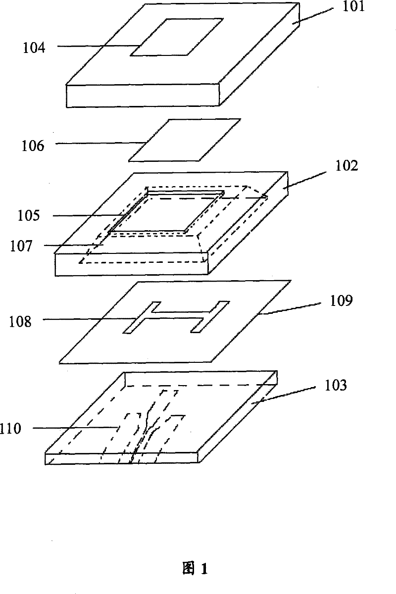
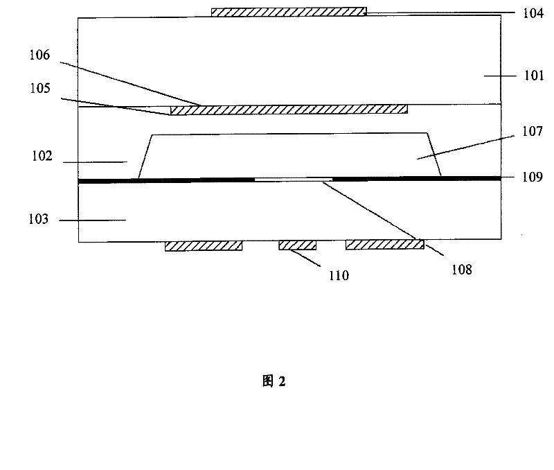
[0039] figure 1 It is a layered perspective view of an embodiment of the present invention. The MEMS 3-layer stacked millimeter wave antenna provided by the embodiment of the present invention includes an upper dielectric substrate (101), a middle dielectric substrate (102) and a lower dielectric substrate (103), the upper dielectric substrate (101) The material is glass, the material of the middle dielectric substrate (102) is high resistance silicon, the material of the lower dielectric substrate (103) is high resistance silicon, and the upper surface of the upper dielectric substrate (101) is deposited There is metal and is etched to form a first metal radiation patch (104), and the upper surface of the middle layer dielectric substrate (102) is etched with a shallow pool (105) where metal is deposited and etched to form a second metal rad...


PUM

PropertyMeasurementUnit
depthaaaaaaaaaa
thicknessaaaaaaaaaa
electrical conductivityaaaaaaaaaa

Abstract

The micro-electromechanical stacked millimeter-wave antenna provided by the present invention includes an upper dielectric substrate, a middle dielectric substrate and a lower dielectric substrate, the upper surface of the upper dielectric substrate is deposited with metal and etched to form a first metal radiation patch , the upper surface of the middle dielectric substrate is deposited with metal and etched to form a second metal radiation patch, the upper surface of the lower dielectric substrate is deposited with metal and etched to form a ground plane with an aperture coupling gap, the lower layer Metal is deposited on the lower surface of the dielectric substrate and etched to form a FGCPW-MS feeder or MS feeder, and the upper dielectric substrate, middle dielectric substrate and lower dielectric substrate are integrated through a MEMS bonding process. The antenna has a small geometry, light weight and is easy to further integrate.

Description

technical field [0001] The invention relates to the field of antennas, in particular to micro-electromechanical laminated millimeter-wave antennas. Background technique [0002] The development and maturity of microwave integration technology and the emergence of various low-loss dielectric materials ensure the manufacturing process of microstrip antennas and reduce manufacturing costs. With the application of computer-aided design analysis software, the design of microstrip antennas is easier ,more reliable. The maturity of materials, technology, and design makes microstrip antennas small in size, light in weight, low in profile, easy to conform, and low in cost. They are widely used in many fields such as satellite communications, radar, remote sensing and telemetry, navigation, and biomedical systems. However, the microstrip antenna also has two defects of narrow operating frequency band and low radiation efficiency, which greatly affect the performance of the microstrip...

Claims


Application Information

Patent Timeline
Patent Type & Authority Patents(China)
IPC IPC(8): H05K3/06H01Q1/38B81C1/00
Inventor 朱健侯芳郁元卫
Owner NO 55 INST CHINA ELECTRONIC SCI & TECHNOLOGYGROUP CO LTD
Why Eureka
Try Eureka