Making method for micro-hole vertical cavity radiation laser

A vertical cavity surface emission, laser technology, applied in lasers, laser parts, semiconductor lasers, etc., can solve the problems of low yield, poor process repeatability, short device life and so on

Inactive Publication Date: 2008-03-19
INST OF SEMICONDUCTORS - CHINESE ACAD OF SCI
View PDF0 Cites 8 Cited by
  • Summary
  • Abstract
  • Description
  • Claims
  • Application Information

AI Technical Summary

Problems solved by technology

[0004] However, since the preparation of VASL needs to etch tiny holes on the active area, and the size of the active area is very small, it is difficult to control the accurate positioning of the small holes, and the repeatabili

Method used


Image

  • Making method for micro-hole vertical cavity radiation laser
  • Making method for micro-hole vertical cavity radiation laser

Examples


Embodiment Construction

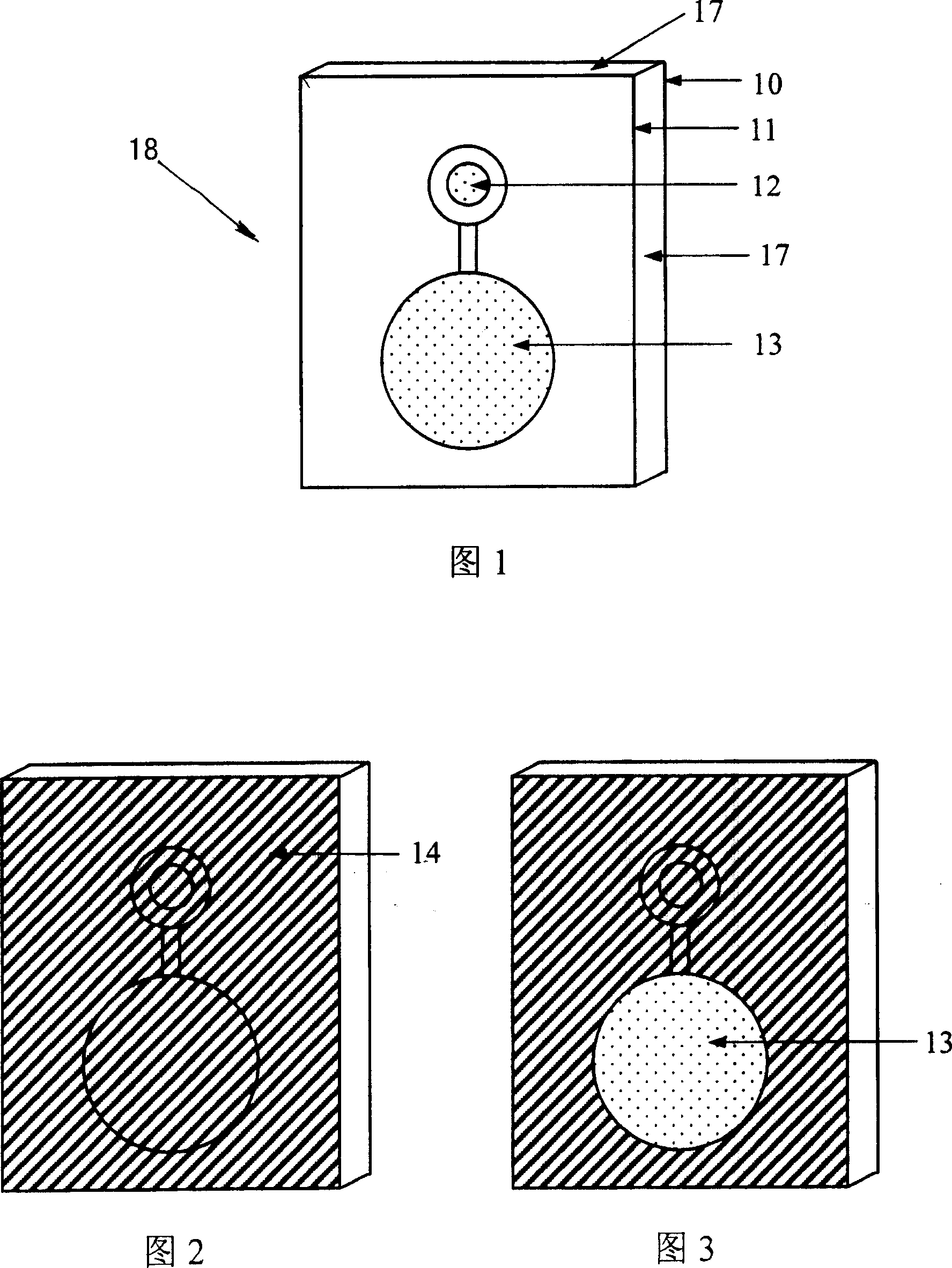
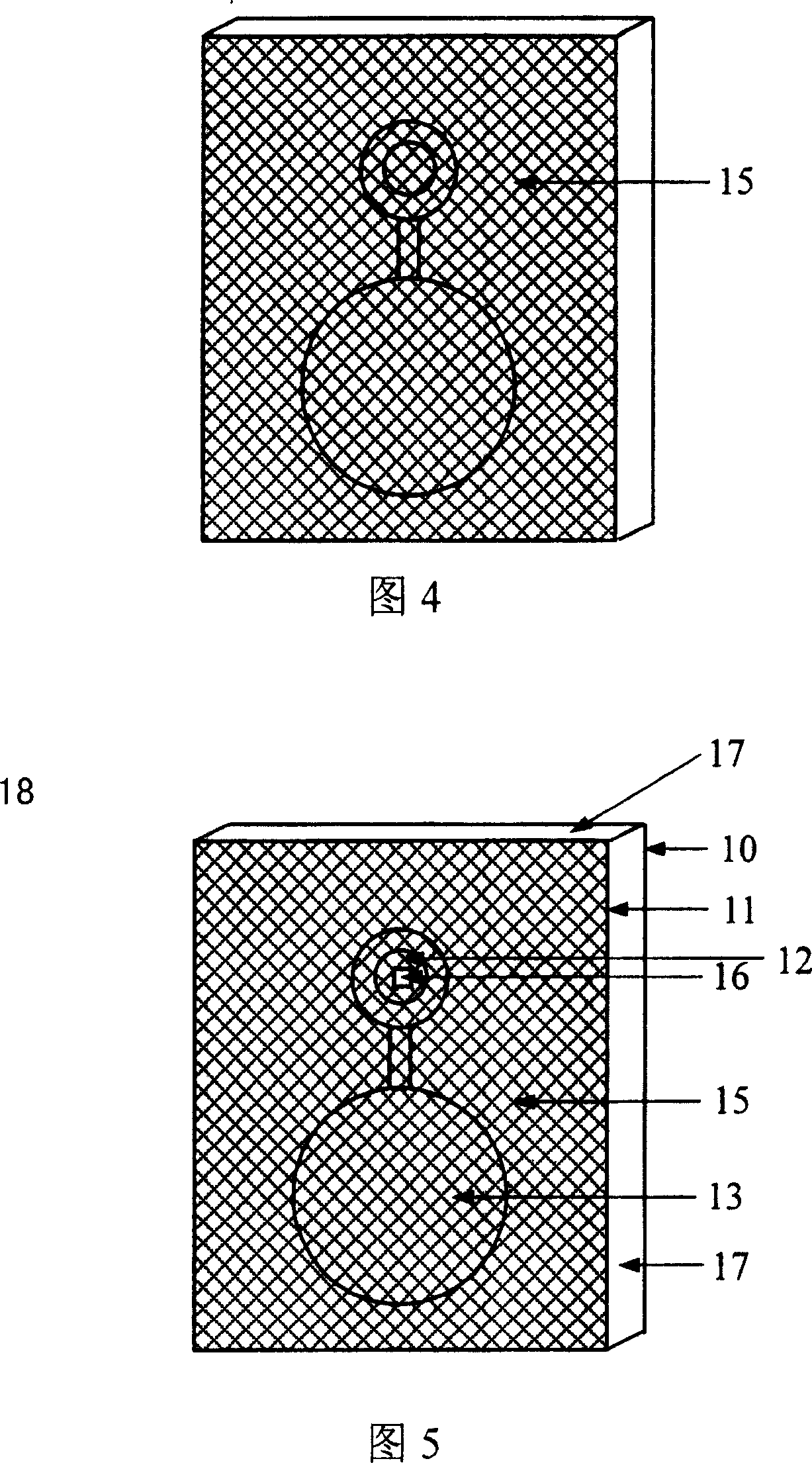
[0026] Please refer to Fig. 1-shown in Fig. 5, a kind of micro hole vertical cavity surface emitting laser of the present invention, comprises the following steps:

[0027] (1) Deposit an anti-reflection film 14 by electron cyclotron resonance plasma chemical vapor deposition (ECR plasma CVD) on the light exit cavity surface 11 of a common VCSEL (Fig. 1), as shown in Fig. 2, the material is SiO 2 and SiN x mixture, or for Al 2 o 3 , MgF and other materials, the thickness is 200nm-400nm. The anti-reflection film 14 is used as an insulating film to avoid direct contact between the metal and the light exit cavity surface 11 in the next step, thereby protecting the light exit cavity surface 11 .

[0028] (2) Etching away the anti-reflection film 14 on the P-surface electrode 13 by using a focused ion beam system, as shown in FIG. 3 , so that the P-surface electrode 13 and the N-surface electrode 10 can form a current injection channel. The etching time is 30s-120s.

[0029] (...


PUM

PropertyMeasurementUnit
Thicknessaaaaaaaaaa
Thicknessaaaaaaaaaa
Thicknessaaaaaaaaaa

Abstract

A method for preparing microporous vertical cavity surface emitting laser comprise the following steps: (1) collecting a common vertical cavity surface emitting laser comprising a N-electrode, an emitting cavity surface, an emitting hole, and a P-electrode; (2) fabricating an anti-reflection film on the emitting cavity surface of the common vertical cavity surface emitting laser; (3) etching the anti-reflection film on the P-electrode by using the focused ion beam etching technique; (4) fabricating a metal film on the anti-reflection film of the emitting cavity surface and the P-electrode; and (5) etching the micropores with subwavelength on the emitting hole to finish the preparation of the microporous vertical cavity surface emitting laser.

Description

technical field [0001] The invention relates to a preparation method of a semiconductor laser, in particular to a preparation method of a microhole vertical cavity surface emitting laser. Background technique [0002] Current optical data storage systems, such as CD or DVD, are far-field storage systems, and their storage density is limited due to the limitation of diffraction limit. Utilizing the evanescent wave in the near-field of the light source can break through the limitation of the diffraction limit and greatly increase the storage density. Therefore, high-density optical data storage has become a large field of near-field optical applications. If a tiny light source that breaks through the diffraction resolution limit can be manufactured, it will be a great impetus to the application fields such as micro-area imaging, micro-area detection and nano-lithography. In this context, near-field optics has developed rapidly. Near-field data storage has become one of the m...

Claims


Application Information

Patent Timeline
IPC IPC(8): H01S5/183
Inventor 高建霞宋国峰甘巧强陈良惠
Owner INST OF SEMICONDUCTORS - CHINESE ACAD OF SCI
Why Eureka
Try Eureka