

High speed deposition micro crystal silicon solar battery P/I interface processing method
A technology of solar cells and processing methods, which is applied to circuits, electrical components, sustainable manufacturing/processing, etc., can solve the problems of increasing the P/I interface defect state and the thickness of the amorphous incubation layer, so as to improve battery efficiency and reduce interface state, reducing the effect of the incubation layer
- Summary
- Abstract
- Description
- Claims
- Application Information
AI Technical Summary
Problems solved by technology
Method used
Image

Examples
Embodiment 1
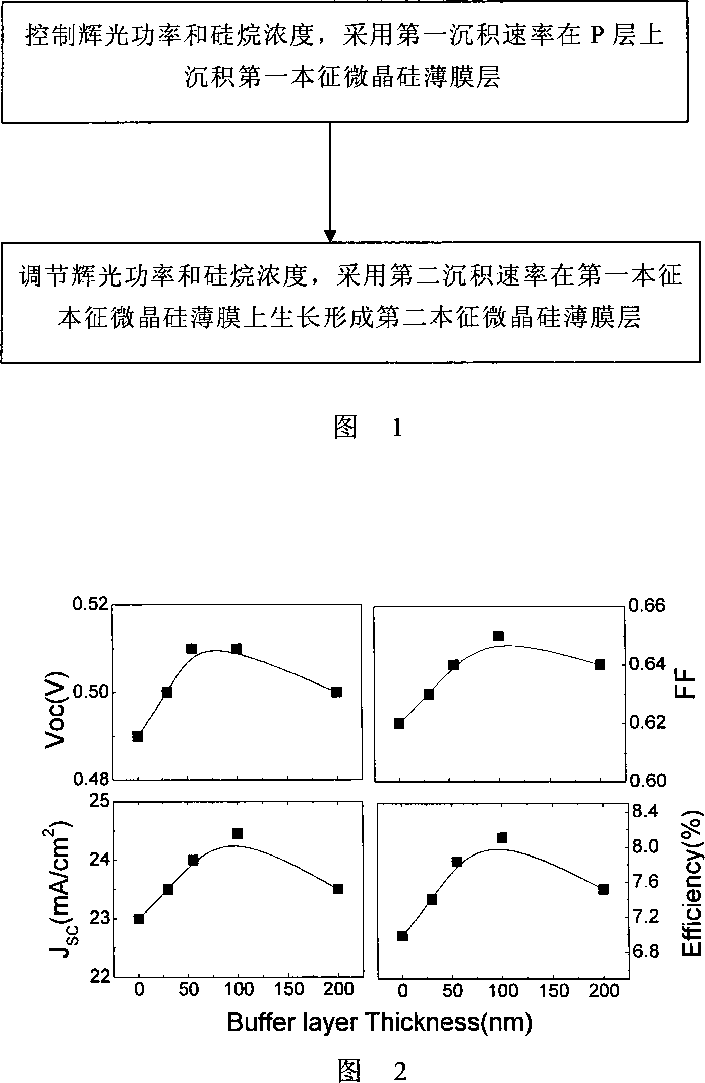
[0025] Embodiment 1, the preferred implementation conditions of the present invention are as follows: the substrate is placed in the reaction chamber, the air pressure in the reaction chamber is maintained at 1.6 torr, and the electrode distance is 12 mm. Power on to start deposition, first set the glow power to 25W, the silane concentration to 3%, the first deposition rate under this condition is about 3 / s, keep the first deposition rate for 5 minutes and 30 seconds, and form the first intrinsic microcrystalline silicon thin film layer with low defect and high crystallization of about 100nm; 50W, silane concentration is 5%, the second deposition rate under this condition is about 8.5 / s, maintain the second deposition rate for 27 minutes, and form a second intrinsic microcrystalline silicon film layer of about 1400 nm. It can be seen from Fig. 2 that the cell efficiency with the low-velocity interface layer with 100nm low defect and high crystallization is increased by ab...
Embodiment 2
[0026] Embodiment 2, if only using the second deposition rate to deposit the intrinsic microcrystalline silicon thin film, the corresponding intrinsic microcrystalline silicon thin film layer thickness in Figure 2 is 0nm, that is, the implementation conditions without the low-speed intrinsic microcrystalline silicon thin film layer are as follows: The substrate was placed in the reaction chamber, the air pressure in the reaction chamber was kept at 1.6 torr, and the electrode distance was 12 mm. The glow power is set to 50W, the silane concentration is 5%, and the deposition rate under these conditions is about 8.5 / s, keep the deposition rate for 29 minutes (time), and form an intrinsic microcrystalline silicon thin film layer of about 1500 nm (thickness). It can be seen from Figure 2 that the cell efficiency without the low-speed intrinsic microcrystalline silicon thin film layer is the lowest relative to the cell efficiency with the low-speed intrinsic microcrystalline sil...
Embodiment 3
[0027] Embodiment 3, if the thickness of the first intrinsic microcrystalline silicon film deposited by the first deposition rate is thicker, the implementation conditions are as follows: the substrate is placed in the reaction chamber, the air pressure in the reaction chamber is maintained at 1.6torr, and the electrode The distance is 12mm. Power on to start deposition, first set the glow power to 25W, the silane concentration to 3%, the first deposition rate under this condition is about 3 / s, the first deposition rate is maintained for 11 minutes, and a first intrinsic microcrystalline silicon thin film layer with a thickness of about 200 nm and low defects and high crystallization is formed. Then when other process conditions remain unchanged, only the glow power is changed to 50W, the silane concentration is 5%, and the second deposition rate under this condition is about 8.5 / s, maintain the second deposition rate for 25 minutes, and form a second intrinsic microcryst...
PUM
| Property | Measurement | Unit |
|---|---|---|
| thickness | aaaaa | aaaaa |
| thickness | aaaaa | aaaaa |
| thickness | aaaaa | aaaaa |
Abstract
Description
Claims
Application Information