
White light LED with modified structure
A technology of light-emitting diodes and white light, which is applied in the direction of optical elements used to change the spectral characteristics of emitted light, semiconductor devices of light-emitting elements, light sources, etc., and can solve problems such as reduced luminous flux, changed color temperature, reduced luminous efficiency and lifespan, etc., to achieve The light intensity and color temperature are stable, the working life is extended, and the service life is extended
- Summary
- Abstract
- Description
- Claims
- Application Information
AI Technical Summary
Problems solved by technology
Method used
Image

Examples
Embodiment 1
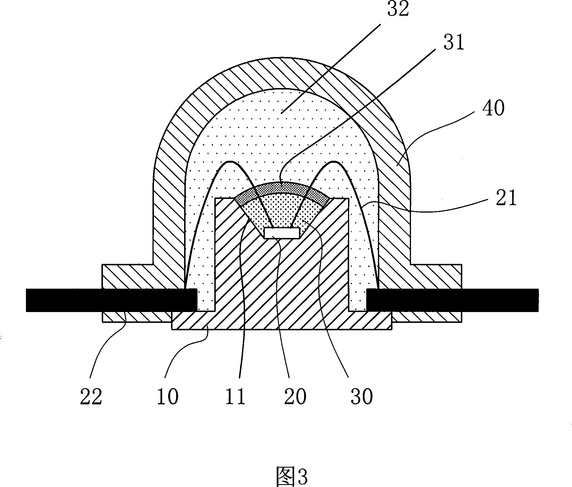
[0025] Embodiment 1: referring to Fig. 3: the white light light-emitting diode of structural improvement, is that the positive and negative electrodes on the light-emitting diode chip 20 are drawn out with lead wire 21 respectively and are connected with the lead pin 22 that extends to outside the lens cover 40, and the lens cover 40 can cover the wafer 20, and at least one wafer 20 is fixed on at least one cup-shaped groove or platform 11 on the base 10, and a light-transmitting, heat-insulating medium 30 is provided on the outer surface of the wafer 20, and the medium 30 A layer of phosphor powder 31 is arranged on the outer surface of the body.
[0026] The aforementioned chip 20 is a blue light chip.
[0027] The above-mentioned medium 30 is made of optical glass, optical plastic, silica gel, epoxy resin, or ceramic material that is heat-insulating, light-transmitting, and UV-resistant.
[0028] The above phosphor powder 31 is disposed on the outer surface of the medium 3...
Embodiment 2
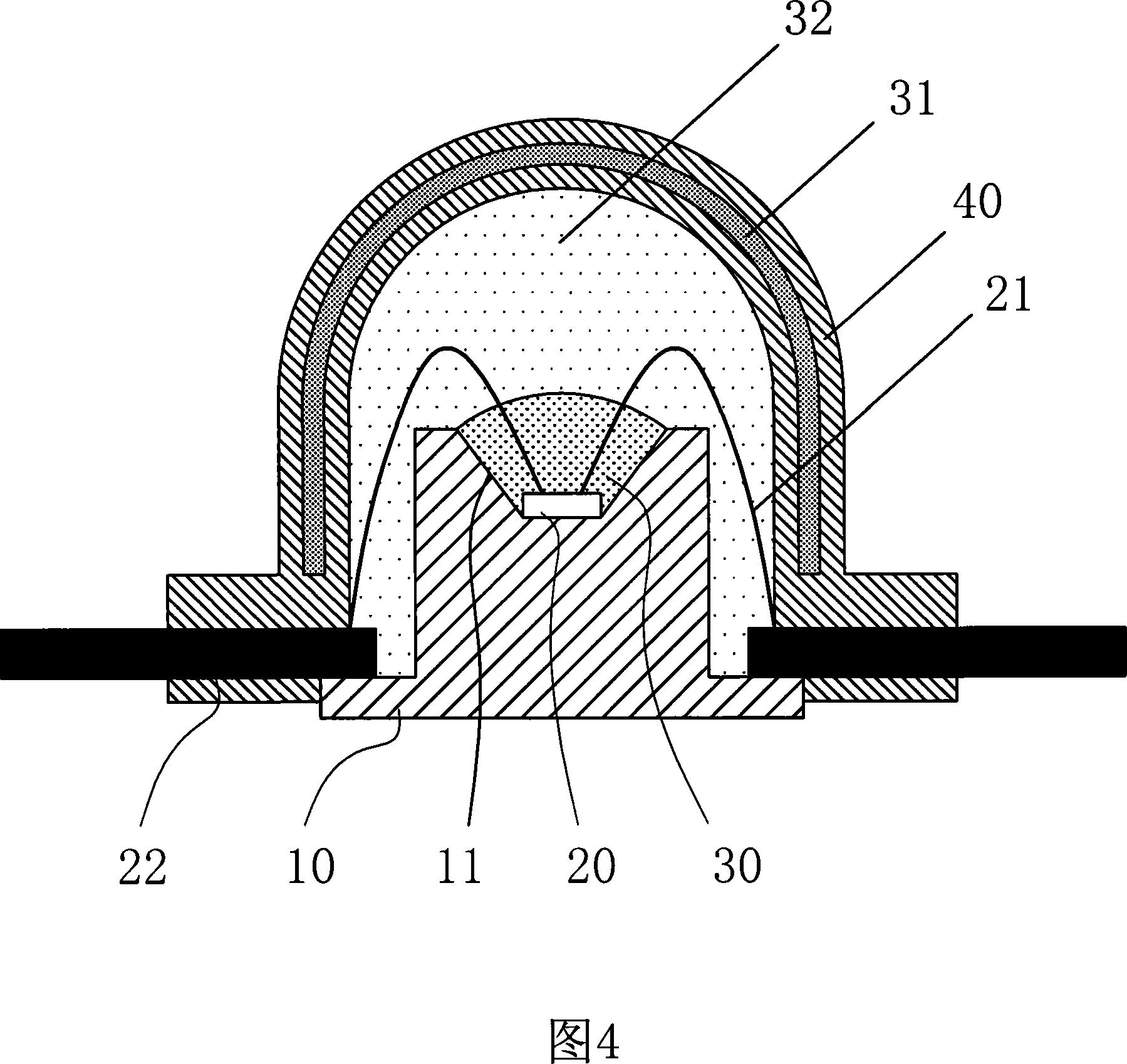
[0032] Embodiment 2: Referring to Fig. 4: the basic structure is the same as that of Embodiment 1, except that the above-mentioned layer of fluorescent powder 31 is arranged on the lens cover 40, that is, in the interlayer of the lens cover 40, of course, the above-mentioned fluorescent powder 31 can also be provided On the inner surface of the lens cover 40 , 41 or on the outer surface of the lens cover 40 , 41 or mixed in the material from which the lens cover 40 , 41 is made.
Embodiment 3
[0033] Embodiment 3: See Figures 5-6: the base 10, wafer 20, cup-shaped groove or platform 11, medium 30, inert gas 32, lead wire 21 and guide pin 22 are basically the same as those in Embodiment 1 or Embodiment 2. , but a plurality of LED lamp assemblies are installed in a metal box body 50, and the upper part of the box body 50 is sealed with a flat lens cover 41, and a layer of phosphor powder 31 is arranged in the interlayer of the lens cover 41. Of course, it can also be like Like embodiment 1 and embodiment 2, fluorescent powder 31 is arranged on the outer surface of medium 30 or the inner surface of lens cover 41 or the outer surface of lens cover 41 or is mixed in the material that makes lens cover 41, positive and negative electrode respectively The lead wires 21 are used to lead out and connect in series with the guide pins 22 respectively. Of course, the number of LEDs can be designed according to the demand of the light intensity. Since the phosphor 31 is insulated ...
PUM
 Abstract
Description
Claims
Application Information