Production method for oxide luminescent layer in inorganic electroluminescence display device

A production method and oxide technology, applied in electroluminescence light source, electric light source, light source and other directions, can solve the problems of high target production cost, difficult composition adjustment, long cycle, etc., saving time and material cost, composition adjustment Easy, short cycle effects

Inactive Publication Date: 2008-05-07
INESA ELECTRON
View PDF0 Cites 5 Cited by
  • Summary
  • Abstract
  • Description
  • Claims
  • Application Information

AI Technical Summary

Problems solved by technology

[0004] The object of the present invention is to provide a kind of preparation method of the oxide light-emitting layer in the inorganic electroluminescent display, described this method will solve the problem in the preparation method of the oxide light-emitting layer in the inorganic electroluminescent display in the prior art In the sintering process of ceramic targets, the technical problems of high cost, long period, and easy fragmentation during sintering, at the same time, it is necessary to solve the technical problems of large-size targets that require splicing of multiple targets and high cost, as well as the production of new targets. Technical problems of high cost, long period, and difficult adjustment of components

Method used


Image

  • Production method for oxide luminescent layer in inorganic electroluminescence display device
  • Production method for oxide luminescent layer in inorganic electroluminescence display device
  • Production method for oxide luminescent layer in inorganic electroluminescence display device

Examples


Embodiment 1

[0030] Mix manganese-doped zinc silicate (green fluorescent powder), zinc oxide (purity 99.99%), germanium oxide (purity 99.999%), and manganese oxide (purity 99.99%) according to the molar ratio of 1:1.92:1:0.08. , sprayed onto the oxygen-free copper backplane with argon plasma, and the thickness of the green ceramic target was 1 mm after spraying.

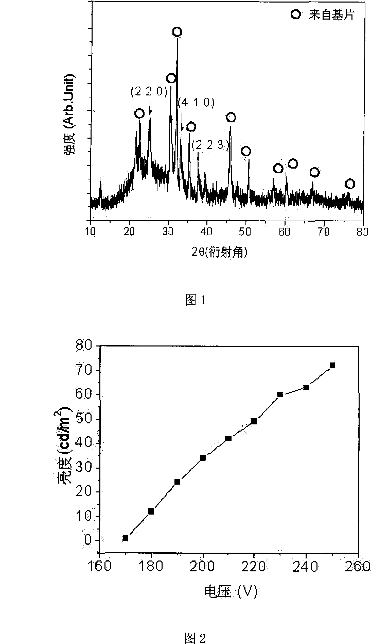
[0031] A lower dielectric layer, barium strontium titanate, is sputter deposited on the transparent lower electrode ITO on the TFT-LCD glass substrate, with a thickness of 300 nanometers. Then, a 400-nm green EL emitting layer was sputtered on the lower dielectric layer of barium strontium titanate with the spraying target made by the above method. The sputtering condition of the light-emitting layer is: the background vacuum is 2.7×10 -3 Pa, Ar / O 2 The ratio is 9:1, the sputtering pressure is 0.1Pa, the substrate temperature is 200°C, the target base distance is 5cm, and the sputtering power density is 8.8W / cm 2 . After sput...

Embodiment 2

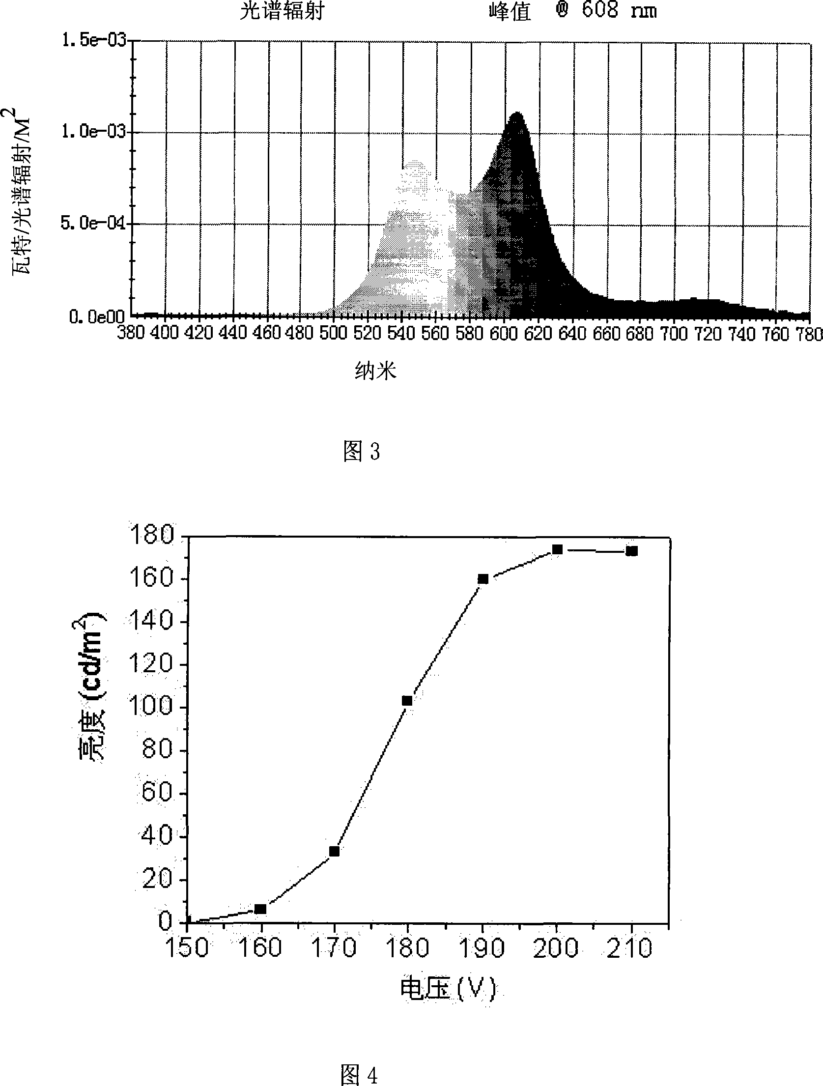
[0033] The preparation method of the spraying target is the same as that of Example 1, but before spraying, the green light powder is mixed evenly and then pre-sintered in the air at 1200°C for 4 hours. This is to make each component react and make it more uniform and stable. . The structure of the fabricated green EL device is the same as that in Example 1. The thickness of the light-emitting layer is 400 nanometers, and the sputtering condition: the background vacuum is 2.7×10 -3 Pa, Ar / O 2 The ratio is 9:1, the sputtering pressure is 2Pa, the substrate temperature is 200°C, the target base distance is 5cm, and the sputtering power density is 8.8W / cm 2 . Annealing is carried out after sputter coating, and the annealing conditions are the same as in Example 1. What Fig. 4 shows is the luminance-voltage curve of this green light EL device, test condition is identical with embodiment 1, what Fig. 5 shows is this green light EL device when applying the electroluminescence sp...

Embodiment 3

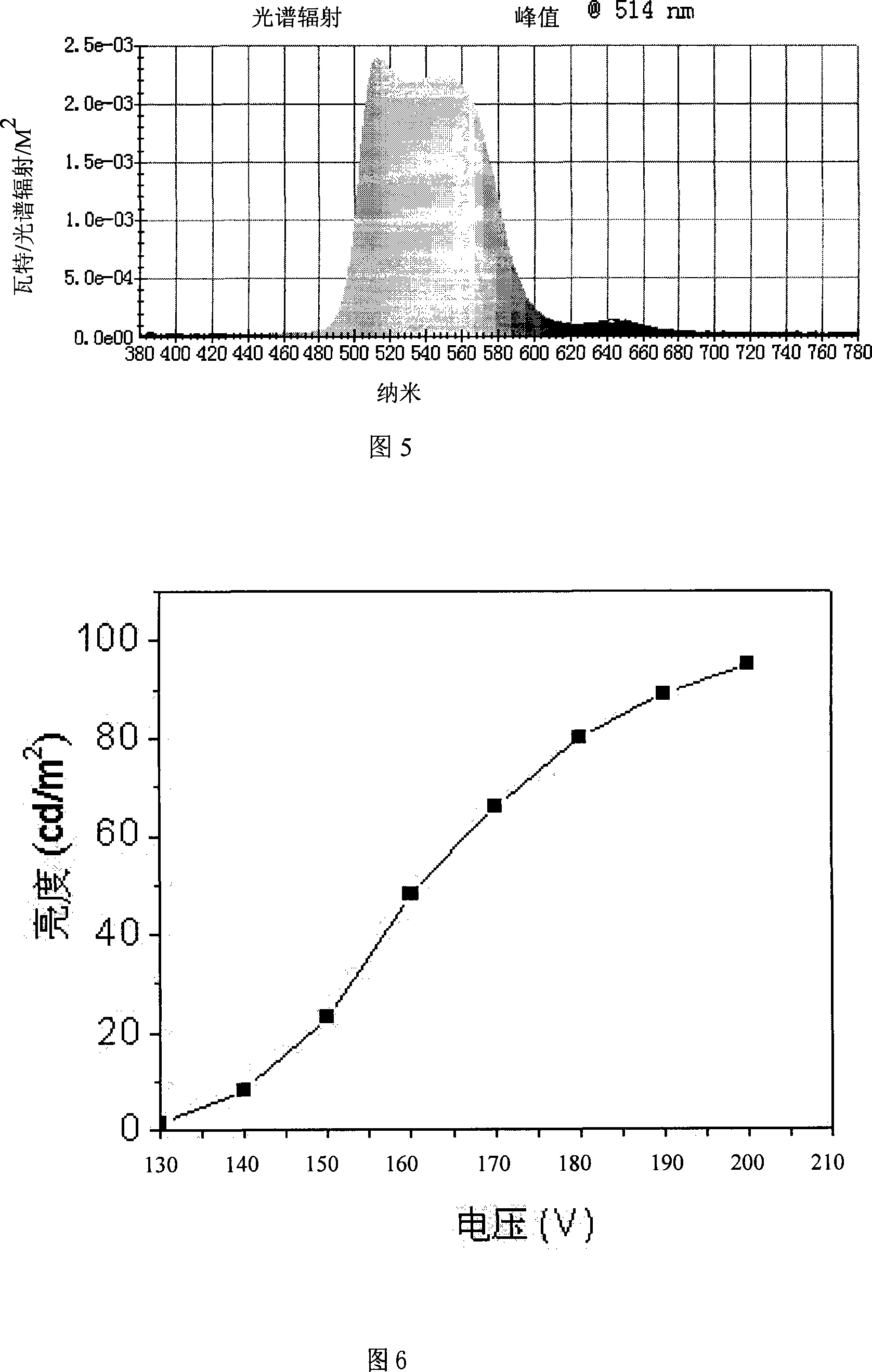
[0035] The preparation method of the spraying target is the same as that of Example 2, and the structure of the fabricated green light device and the sputtering conditions of the light-emitting layer are the same as those of Example 2. The luminescent layer was annealed in a vacuum annealing furnace at 700°C for one hour, and oxygen was introduced to 1.2*10 during the annealing process. -2 Pa. What Fig. 6 shows is the luminance-voltage curve of this green light EL device, and test condition is identical with embodiment 1, and what Fig. 7 shows is this green light EL device when applying 200V AC pulse voltage, and the corresponding color coordinates are (x=0.428, y=0.550).


PUM

PropertyMeasurementUnit
thicknessaaaaaaaaaa
thicknessaaaaaaaaaa
thicknessaaaaaaaaaa

Abstract

The present invention discloses the production method of the oxide luminous layer in a non-organic electroluminescent display, which belongs to the manufacturing technical field of the non-organic electroluminescent display driven by alternating current. The method of the present invention is that the corresponding oxide powder is directly sprayed and coated on a metal backboard to make a ceramic target. The ceramic target is sputtered on a plating film to form an oxide luminous layer film, which is applied to the non-organic electroluminescent display. With the present invention, the production cost of a large-size target used for sputtering and aggrading a large-area oxide luminous film; the crack in the ceramic target production agglutinating process is avoided; the probability of the crack in the target using process is reduced; the target component is much easier to be adjusted; and the research and development and the production costs of the display are reduced.

Description

Technical field: [0001] The invention belongs to the technical field of flat panel display, and in particular relates to an inorganic electroluminescent display, in particular to a method for manufacturing an oxide luminescent layer in an inorganic electroluminescent display. Background technique: [0002] Inorganic electroluminescent (EL) flat panel displays have the characteristics of all solid state, light weight, thin thickness, large viewing angle, and simple structure. They can be used in harsh environments such as low temperature and vibration, and have broad application prospects. Inorganic electroluminescent displays generally use sulfides or oxides as the light-emitting layer, among which oxides are used as the light-emitting layer, which has the advantages of simple film manufacturing process, strong moisture resistance of the device, rich colors, and easy mass production. In order to obtain luminous efficiency that meets practical requirements, oxides with multi-...

Claims


Application Information

Patent Timeline
Patent Type & Authority Applications(China)
IPC IPC(8): H05B33/10H05B33/14
Inventor 肖田楼均辉陈晨曦周团团张羿
Owner INESA ELECTRON
Why Eureka
Try Eureka