High, depth and width three-dimensional uprightness interconnect and realization method of three-dimensional integrate circuit

An integrated circuit and vertical interconnection technology, applied in the direction of circuits, electrical components, electric solid devices, etc., can solve the problems of difficulty in ensuring the insulation effect of interconnecting lines, limiting interconnection line density, and difficulty in the growth of insulating layers. High-density 3D vertical interconnects, avoiding voids and gaps, and eliminating dependencies

Inactive Publication Date: 2008-05-14
TSINGHUA UNIV
View PDF0 Cites 30 Cited by
  • Summary
  • Abstract
  • Description
  • Claims
  • Application Information

AI Technical Summary

Problems solved by technology

This method is easy to fill through holes, but in order to ensure the operability of the semiconductor wafer, the thickness of a single-layer semiconductor wafer is often more than 200 microns, even if the aspect ratio of the vertical interconnection line is as high as 20, the lateral dimension of the interconnection line is too large. Above 10 microns, limits the improvement of interconnect line density
[0008] One solution is to make an electroplating seed layer on the front side of the semiconductor wafer, and then conduct a thinning treatment on the semiconductor wafer through temporary bonding of the auxiliary wafer, and then perform deep reactive ion etching (DRIE) to o

Method used


Image

  • High, depth and width three-dimensional uprightness interconnect and realization method of three-dimensional integrate circuit
  • High, depth and width three-dimensional uprightness interconnect and realization method of three-dimensional integrate circuit
  • High, depth and width three-dimensional uprightness interconnect and realization method of three-dimensional integrate circuit

Examples


Embodiment Construction

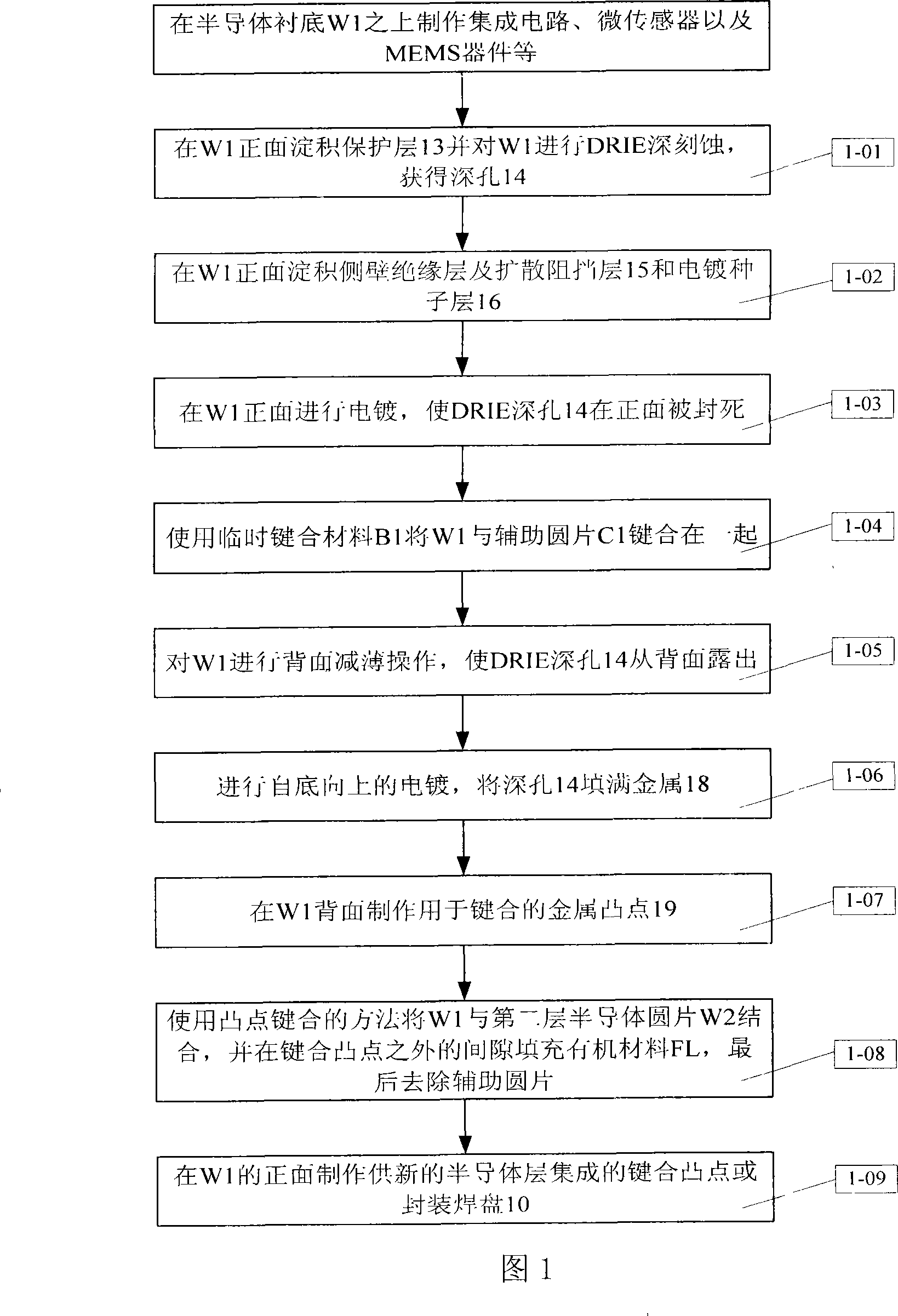
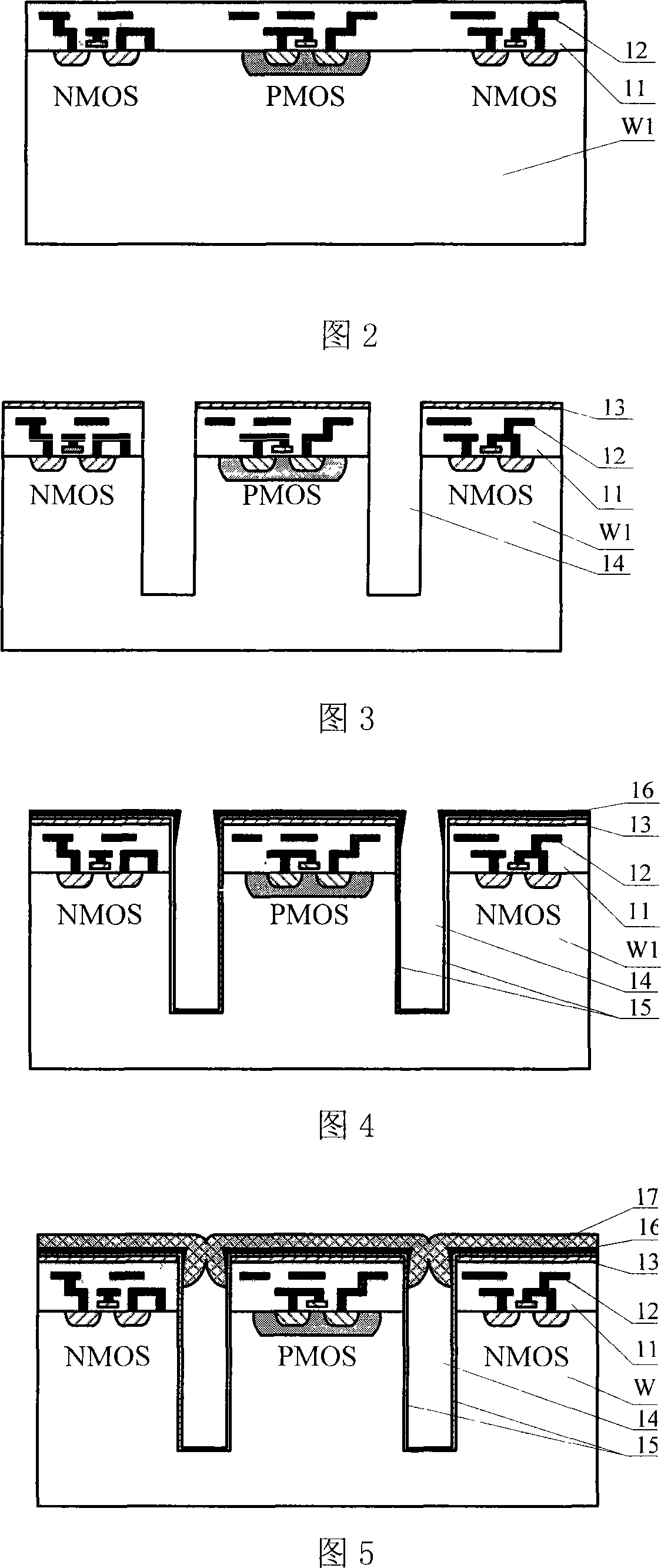
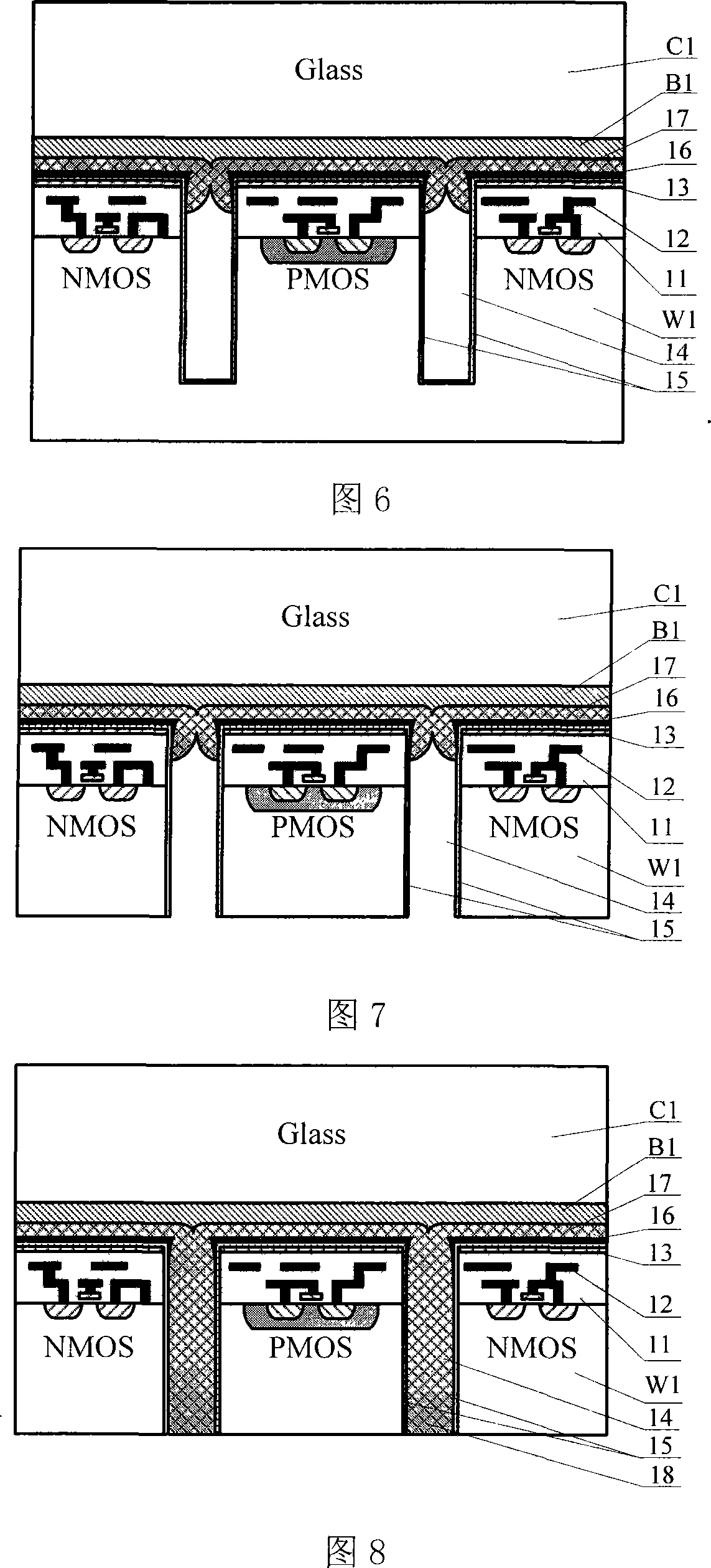
[0037]The present invention provides a high aspect ratio three-dimensional vertical interconnection and three-dimensional integrated circuit realization method. For the purpose of the present invention, the present invention is achieved by first deep etching by DRIE and then bonding the auxiliary wafer and thinning the device wafer. Consistent etching of through holes with different aspect ratios and avoiding lateral etching, using double-sided deposition of insulating layer, diffusion barrier layer and electroplating seed layer to solve the internal insulating layer, diffusion barrier layer and electroplating seed layer of high aspect ratio through holes The problem of difficult deposition, and the bottom-up electroplating process to fill the through holes to overcome the problem that the single-sided Damascus electroplating high aspect ratio structure is prone to gaps.

[0038] The embodiments of the present invention will be described in further detail below in conjunction with...


PUM


Abstract

The invention discloses a method for implementing a high aspect ratio three-dimensional vertical interconnection and a three-dimensional integrated circuit, which belongs to fields of semiconductor manufacture technology and micro-sensor manufacture technology. The method includes the following steps: carrying out a deep reactive ion etching at the front side of a semiconductor wafer with a prepared plant integrated circuit or a prepared micro-sensor, and gaining deep pores; precipitating a insulation layer, a diffusion barrier and a plating seed layer at the front side; temporarily bonding the semiconductor wafer plating face and an assistant wafer, thinning the back of the semiconductor wafer in such a manner that DRIE deep pores are exposed from the back; precipitating the insulation layer, the diffusion barrier and the plating seed layer at the back side; carrying out the plating upwards from the bottom and filling the DRIE deep pores to form the high aspect ratio three-dimensional vertical interconnection; removing the assistant wafer and implementing the vertical integration of two layers of wafers; and repeating the steps above and implementing the three-dimensional integrated circuit with more layers. The invention reduces difficulty of the process for filling the high aspect ratio through-hole, simplifies the manufacturing process, and ensures the yield.

Description

Technical field [0001] The invention belongs to the technical field of semiconductor and micro-sensor manufacturing, and particularly relates to a high-aspect-ratio three-dimensional vertical interconnection and three-dimensional integrated circuit realization method using three-dimensional integrated circuit manufacturing technology. Background technique [0002] The continuous shrinking of integrated circuit devices has continuously improved the integration level. At present, more than 1 billion transistors can be integrated per square centimeter of chip area, and the total length of metal interconnection lines has reached tens of kilometers. This not only makes the wiring extremely complicated, but more importantly, the delay, power consumption, and noise of the metal interconnection increase with the decrease of the feature size, especially the RC delay of the global interconnection, which seriously affects the integrated circuit. performance. In addition, dynamic power consu...

Claims


Application Information

Patent Timeline
IPC IPC(8): H01L21/60
CPCH01L2224/16145
Inventor 王喆垚宋崇申陈倩文蔡坚刘理天
Owner TSINGHUA UNIV
Why Eureka
Try Eureka