White light organic electroluminescent device and method for fabricating the same based on fluorochrome

A technology of electroluminescent devices and fluorescent dyes, applied in the direction of electric solid devices, semiconductor/solid device manufacturing, electrical components, etc., to achieve the effects of high brightness, good stability, high brightness and efficiency

Inactive Publication Date: 2008-05-14
中科应化(长春)科技有限公司
View PDF2 Cites 11 Cited by
  • Summary
  • Abstract
  • Description
  • Claims
  • Application Information

AI Technical Summary

Problems solved by technology

However, judging from the current development, there is still a long way to go for large-scale commercial application of white light organic electroluminescent devices, and there are many problems to be solved

Method used


Image

  • White light organic electroluminescent device and method for fabricating the same based on fluorochrome
  • White light organic electroluminescent device and method for fabricating the same based on fluorochrome
  • White light organic electroluminescent device and method for fabricating the same based on fluorochrome

Examples


Embodiment 1

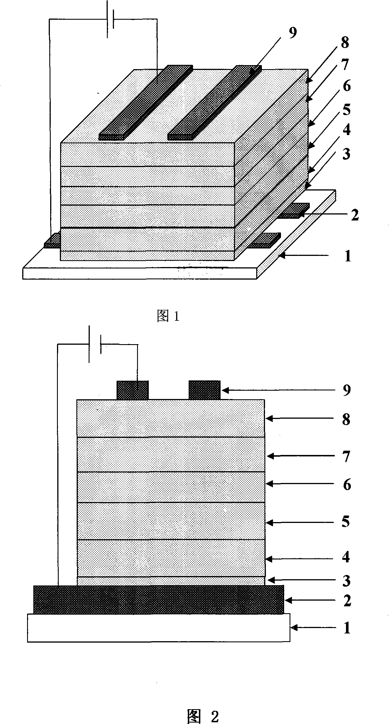
[0035] The ITO on the ITO glass was first photoetched into electrodes with a width of 4 mm and a length of 30 mm, then cleaned, dried with nitrogen, and treated with oxygen plasma for 2 minutes. In a vacuum of 1 to 5 x 10 -4 In Pa's coating system, MoO with a thickness of 8 nanometers is sequentially evaporated on the treated ITO electrode. 3 , 150 nanometer thick NPB hole transport layer, 20 nanometer DCJTB doped NPB red light emitting layer with a weight ratio of 0.5%, 3 nanometer C545T with a weight ratio of 0.5% doped Alq 3 The green light-emitting layer of 40 nanometers of DSA-Ph doped blue light-emitting layer of MADN with a weight ratio of 0.5%, the BAlq of 10 nanometers 3 The electron transport layer and the LiF interface layer of 1 nanometer, and finally a metal Al electrode with a width of 4 mm, a length of 30 mm and a thickness of 200 nanometers crossed with ITO is evaporated on LiF, and the structure is ITO / MoO 3 / NPB / DCJTB:NPB / C545T:Alq 3 / DSA-Ph:MADN / BAlq 3 / ...

Embodiment 2

[0037] The ITO on the polycarbonate substrate was first photoetched into electrodes with a width of 4 mm and a length of 30 mm, then cleaned, dried with nitrogen, and treated with oxygen plasma for 2 minutes. In a vacuum of 1 to 5 x 10 -4 In Pa's coating system, MoO with a thickness of 8 nanometers is sequentially evaporated on the treated ITO electrode. 3 , 70 nanometers thick NPB hole transport layer, 20 nanometers of C545T and DCJTB doped red light-emitting layer of NPB at a concentration of 0.5% and 1% by weight, respectively, 3 nanometers of C545T doped with Alq at a weight ratio of 0.5% 3 Green light-emitting layer, 40 nanometers of DSA-Ph doped MADN blue light-emitting layer with a weight ratio of 0.5%, 10 nanometers of Alq 3 The electron transport layer and the LiF interface layer of 1 nanometer, and finally a metal Al electrode with a width of 4 mm, a length of 30 mm and a thickness of 200 nanometers crossed with ITO is evaporated on LiF, and the structure is ITO / MoO...

Embodiment 3

[0039] Electrode Ag with a width of 4 mm and a length of 30 mm was evaporated on the treated blank glass, and then treated with oxygen plasma for 2 minutes. In a vacuum of 1 to 5 x 10 -4 In Pa's coating system, 20 nanometers thick MoO is sequentially evaporated on the treated Ag electrode. 3 , 150 nanometers thick NPB hole transport layer, 20 nanometers of C545T and DCJTB doped NPB red light-emitting layer with a weight ratio of 0.5% and 1% respectively, 3 nanometers of C545T with a weight ratio of 0.5% doped Alq 3 Green light-emitting layer, 40 nanometers of DSA-Ph doped MADN blue light-emitting layer with a weight ratio of 0.5%, 10 nanometers of Alq 3 The electron transport layer and the LiF interface layer of 1 nanometer, and finally a metal Al electrode with a width of 4 mm, a length of 30 mm, and a thickness of 200 nm crossed with Ag is evaporated on the LiF to prepare a structure of Ag / MoO 3 / NPB / C545T:DCJTB:NPB / C545T:Alq 3 / DSA-Ph:MADN / Alq 3 / LiF / Al organic electrol...


PUM


Abstract

The invention pertains to a white organic light-emitting device based on the fluorescent dye and discloses the preparation method. The method adopts red, green and blue light-emitting structure, takes metal oxide as buffer layer and prepares white organic light-emitting devices with structures of indium tin oxide (ITO) / metal oxide / hole-transporting layer / red light-emitting layer / green light-emitting layer / blue light-emitting layer / electron transporting layer / metal cathode. The prepared devices are driven by direct voltage and emit high-efficient white light; the maximum electroluminescence current efficiency is 20.8cd / A; the maximum electroluminescence (EL) power efficiency is 16lw / W; the maximum luminance is 48000cd / m2 and the devices show simultaneous emission of red, green and blue and stable spectrum when at work.

Description

technical field [0001] The invention relates to a fluorescent dye-based white light organic electroluminescent device and a preparation method thereof. Background technique [0002] Organic electroluminescent display is regarded as the most popular emerging display technology in the flat panel display industry, and has been extensively researched. Compared with inorganic electroluminescent devices, organic electroluminescent devices have a wide range of material selection, can realize full-color display from blue light region to red light region, low driving voltage, high luminous brightness and luminous efficiency, wide viewing angle, and fast response speed. Fast, simple manufacturing process, low cost, and easy to realize large-area and flexible display and many other advantages, so it has developed rapidly in the past 20 years. At present, research in the field of organic light-emitting display devices is no longer limited to academia. Almost all internationally renowne...

Claims


Application Information

Patent Timeline
Patent Type & Authority Applications(China)
IPC IPC(8): H01L51/50H01L51/54H01L51/56
Inventor 马东阁张智强王琦刘一鹏代岩峰游汉
Owner 中科应化(长春)科技有限公司
Why Eureka
Try Eureka