Lndium antimonide opto-electronic sensor array quiescent operating point auto-calibration device

A technology of photoelectric sensor and static working point, which is applied in the field of photoelectric detection technology and electronics, and can solve the problems of consuming manpower and material resources, difficulties, unstable temperature coefficient of sensors, etc.

Inactive Publication Date: 2008-05-21
ANHUI INST OF OPTICS & FINE MECHANICS - CHINESE ACAD OF SCI
View PDF0 Cites 4 Cited by
  • Summary
  • Abstract
  • Description
  • Claims
  • Application Information

AI Technical Summary

Problems solved by technology

[0004] However, in an array detector, especially in an array with a relatively large number of units, it is not feasible mechanically to chop the optical signal, so the method of detecting continuous light is adopted, which requires: 1. The amplifier adopts a DC amplifier, And the magnification is very large (about 5000 times), which means that the temperature change of 0.5 degrees can saturate the amplifier
2. Even if the temperature compensation is carried out, due to the unstable temperature coefficient of each sensor, there must be residual errors that cannot be compensated. In the temperature range of the instrume

Method used


Image

  • Lndium antimonide opto-electronic sensor array quiescent operating point auto-calibration device

Examples


Embodiment Construction

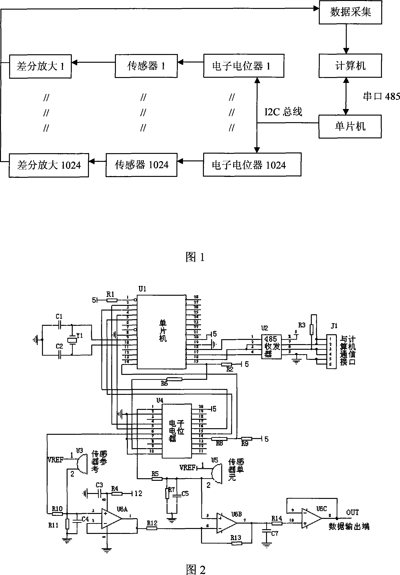
[0014] See Figure 1 and Figure 2.

[0015] In Figure 2, U1 is the PIC16F876A single-chip microcomputer of Microchip Company; U2 is the RS-485 differential bus transceiver SN65LBC184; U3 is the reference of the indium antimonide sensor; U4 is the electronic potentiometer X9241AYP; U5 is the indium antimonide sensor unit; U6 is the operational amplifier.

[0016] The 2(RA0), 3(RA1), 4(RA2), 5(RA3) pins of the microcontroller are respectively connected to the 4(A0), 16(A1), 5(A2), 15(A3) of the electronic potentiometer X9241AYP Pin, as the address line of X9241AYP.

[0017] The 26th pin of the MCU is connected with the 1st pin of SN65LBC184, the 24th pin of the MCU is connected with the 4th pin of SN65LBC184 as the serial port communication line; the 25th pin of the MCU is connected with the 2nd and 3rd pins of the SN65LBC184 as the transceiver control line of the serial port ; R3 is the matching resistor; J1 is the communication interface between the microcontroller and the com...


PUM


Abstract

The invention discloses an automatic adjusting device for the quiescent operation point of an indium antimonide photoelectric sensor array and comprises an indium antimonide photoelectric sensor array. The invention is characterized in that the each indium antimonide photoelectric sensor in the indium antimonide photoelectric sensor array switches in an adjusting branch circuit and the structure of each adjusting branch circuit is as follows that after the standard voltage VREF is outputted through a reference sensor, one way switches to an electric potentiometer through a voltage division circuit and the other way is outputted to a first voltage follower. An address line, a communication clock line and a communication data line are connected between the electric potentiometer and a single chip; the communication connection is established between a collection card and a computer; the communication connection is established between the computer and the single chip. With the automatic adjusting device for quiescent operation point, the sensor array can work naturally in the environment with the temperature range of 30 DEG C below zero to 40 DEG C and the practicality is improved greatly.

Description

technical field [0001] The invention relates to the fields of photoelectric detection technology and electronics, in particular to an automatic calibration device for the static working point of an indium antimonide photoelectric sensor array. Background technique [0002] At present, indium antimonide is a direct semiconductor with a narrow bandgap width of 0.17eV at room temperature, indicating that it has a long-wavelength limit of spectral response greater than 7um, and the response time is an order of magnitude smaller than that of mercury cadmium telluride, reaching 10ns. At the same time, because the detector is made of InSb single crystal, it has stable performance and can work at room temperature without refrigeration. Therefore, the detector is simple in structure, small in size and easy to use, and is an ideal device for mid-infrared detection at present. [0003] However, the temperature coefficient of the indium antimonide photoconductive infrared detector is r...

Claims


Application Information

Patent Timeline
IPC IPC(8): G01J5/24G01J5/02G01J1/44G01J1/02
Inventor 谭逢富侯再红何枫吴毅
Owner ANHUI INST OF OPTICS & FINE MECHANICS - CHINESE ACAD OF SCI
Why Eureka
Try Eureka