A Ge adulterated AZO transparent conductive film and its making method
A transparent conductive film and margin technology, applied to the conductive layer on the insulating carrier, metal/alloy conductors and other directions, can solve the problems of AZO film porosity, loose AZO film, unstable electrical conductivity, etc., to improve electrical conductivity and Visible light transmittance, good adhesion, dense and complete surface
- Summary
- Abstract
- Description
- Claims
- Application Information
AI Technical Summary
Problems solved by technology
Method used
Image
Examples
Embodiment 1
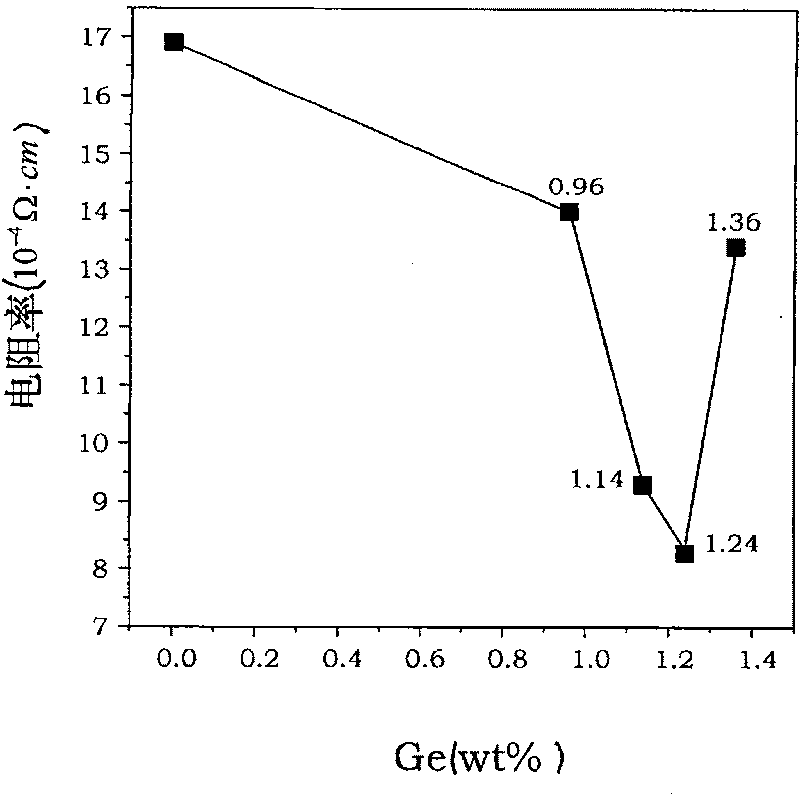
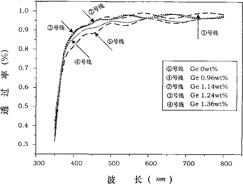
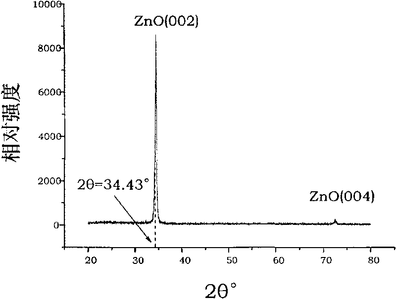
[0029] Example 1: AZO transparent conductive film with a thickness of 750nm and a Ge content of 1.24wt%
[0030] Step 1: Substrate pretreatment
[0031] Select a 15mm×5mm×0.9mm ordinary glass sheet, and ultrasonically clean it in 95% acetone for 10 minutes, then perform ultrasonic surface cleaning in 99% alcohol for 10 minutes, and then blow dry to obtain the substrate;
[0032] Step 2: Select the target
[0033] Select a ZnO target material of φ60mm×5mm, and the ZnO target material contains 2wt% Al 2 o 3 ,, the first target;
[0034] Select a 1mm×1mm×0.2mm Ge sheet with a purity of 99.999%, that is, the second target material, for use;
[0035] The third step: radio frequency magnetron sputtering film formation
[0036] The substrate obtained in the first step is installed on the anode plate of a magnetron sputtering apparatus (JGP560BV type ultra-high vacuum multi-target magnetron sputtering coating machine of China Shenyang Instrument Development Center Co., Ltd.); ...
Embodiment 2
[0049] Example 2: AZO transparent conductive film with a thickness of 500 nm and a Ge content of 0.5 wt %
[0050] Step 1: Substrate pretreatment
[0051] Select a 15mm×5mm×0.9mm ordinary glass sheet, and ultrasonically clean it in 95% acetone for 5 minutes, then perform ultrasonic surface cleaning in 99% alcohol for 5 minutes, and then blow dry to obtain the substrate;
[0052] Step 2: Select the target
[0053] Select a ZnO target material of φ60mm×5mm, and the ZnO target material contains 2wt% Al 2 o3 , the first target;
[0054] Select a 1mm×1mm×0.2mm Ge sheet with a purity of 99.999%, that is, the second target material, for use;
[0055] The third step: radio frequency magnetron sputtering film formation
[0056] The substrate obtained in the first step is installed on the anode plate of a magnetron sputtering apparatus (JGP560BV type ultra-high vacuum multi-target magnetron sputtering coating machine of China Shenyang Instrument Development Center Co., Ltd.);
[...
PUM
| Property | Measurement | Unit |
|---|---|---|
| electrical resistivity | aaaaa | aaaaa |
| electrical resistivity | aaaaa | aaaaa |
| electrical resistivity | aaaaa | aaaaa |
Abstract
Description
Claims
Application Information


