Semiconductor underlay and production method and its application on silicon and extension of insulator

A semiconductor and substrate technology, applied in the field of microelectronics and solid-state electronics, and silicon-based integrated optoelectronic device materials, can solve problems such as harmful device performance

Active Publication Date: 2008-06-11
SHANGHAI SIMGUI TECH +1
View PDF0 Cites 19 Cited by
  • Summary
  • Abstract
  • Description
  • Claims
  • Application Information

AI Technical Summary

Problems solved by technology

[0005] For the process steps of high-temperature strengthening in the prior art, there is a problem that a large amount of residual thermal stress is introduced into the top silicon layer, and the existence of thermal stress will have a harmful impact on the performance of the device, and in the heterogeneous epitaxy process of semiconductor materials, How to release the stress caused by lattice mismatch, the purpose of the present invention is to: provide a semiconductor substrate with embedded hole layer, use the semiconductor substrate as an epitaxial substrate for the epitaxy of gallium nitride, silicon germanium and other materials, and As a support substrate for the fabrication of generalized bonding thinned silicon-on-insulator materials with small residual thermal stress in the top silicon layer of the generalized silicon-on-insulator material

Method used


Image

  • Semiconductor underlay and production method and its application on silicon and extension of insulator
  • Semiconductor underlay and production method and its application on silicon and extension of insulator
  • Semiconductor underlay and production method and its application on silicon and extension of insulator

Examples


Embodiment Construction

[0076] Below in conjunction with accompanying drawing, the semiconductor substrate described in the present invention, the preparation method of semiconductor substrate and the silicon material on thinning insulator and adopting this semiconductor substrate as the epitaxial substrate The specific implementation of the epitaxial gallium nitride material will be described in detail.

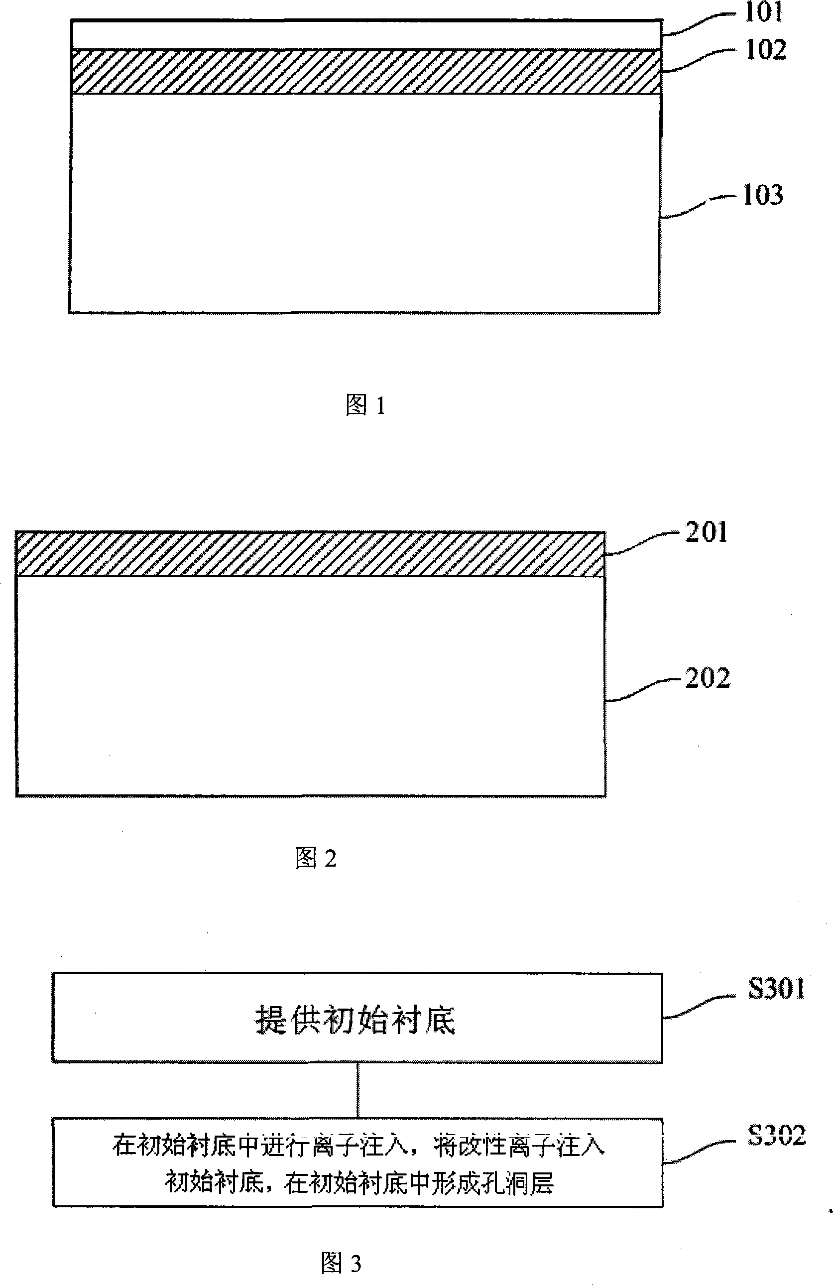
[0077] Firstly, the specific implementation manner of the semiconductor substrate described in the present invention will be introduced. FIG. 1 is a schematic diagram of a first embodiment of a semiconductor substrate, including a cover layer 101 , a hole layer 102 below the cover layer, and a support layer 103 below the hole layer.

[0078] The material of the hole layer 102 is porous silicon or single crystal silicon containing bubbles, the material of the covering layer 101 is single crystal silicon, and the material of the supporting layer 103 is single crystal silicon,

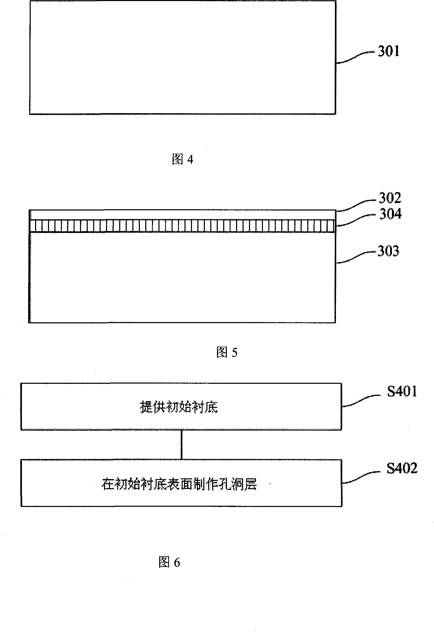
[0079] FIG. 2 is a sc...


PUM

PropertyMeasurementUnit
current densityaaaaaaaaaa
thicknessaaaaaaaaaa
thicknessaaaaaaaaaa

Abstract

The invention relates to a semi-conductor substrate, which comprises a covering layer which is positioned on the top layer and a cave layer which is positioned below the covering layer and a supporting layer which is positioned below the cave layer. The semi-conductor substrate with a special structure is prepared by two methods, that is, an ion injection and an anode oxidization. At the same time, the invention further discloses a method for preparing a silicon material on a generalized bonded thin insulator by the semi-conductor substrate, and a method for using the semi-conductor substrate for material extension as an extending substrate. Compared with the prior art, the invention has the advantage that the cave layer in the semi-conductor substrate can help release interlayer stress, thus acquiring perfect single crystal material.

Description

technical field [0001] The invention belongs to the manufacturing field of microelectronics and solid electronics, and silicon-based integrated optoelectronic device materials. Background technique [0002] Silicon on insulator (that is, SOI-silicon on insulator) has the advantages of high speed, low power, and radiation resistance. It has important application prospects in aerospace, military electronics, portable communications, and automotive electronics. It is considered to be the twenty-first The silicon integrated circuit technology of the century has attracted much attention (J.P.Colinge, Silicon on Insulator Technology, Material to VLSI, Kulwer Academic Publication 1991). With the development of automotive electronic integrated circuits, audio power amplifier integrated circuits, lighting, etc., the demand for power devices is becoming more and more extensive. Because of its good insulation properties, SOI substrates have a particularly promising application prospect...

Claims


Application Information

Patent Timeline
Patent Type & Authority Applications(China)
IPC IPC(8): H01L21/20H01L21/265H01L21/762H01L21/84
Inventor 魏星张苗王曦林成鲁
Owner SHANGHAI SIMGUI TECH
Why Eureka
Try Eureka