Emitting laser for etching top end non-doping intrinsic layer asymmetric metal membrane vertical cavity surface

A vertical cavity surface emission, metal film technology, applied in lasers, laser parts, semiconductor lasers, etc., can solve the problems of inability to achieve a small current aperture, uncontrollable oxidation of small apertures, and limited development, to improve optoelectronic coupling. efficiency, improve luminous efficiency, reduce the effect of area recombination

Inactive Publication Date: 2008-06-18
HEBEI UNIV OF TECH
View PDF2 Cites 12 Cited by
  • Summary
  • Abstract
  • Description
  • Claims
  • Application Information

AI Technical Summary

Problems solved by technology

The use of proton bombardment cannot achieve very small current apertures, and the small apertures of oxid

Method used


Image

  • Emitting laser for etching top end non-doping intrinsic layer asymmetric metal membrane vertical cavity surface
  • Emitting laser for etching top end non-doping intrinsic layer asymmetric metal membrane vertical cavity surface
  • Emitting laser for etching top end non-doping intrinsic layer asymmetric metal membrane vertical cavity surface

Examples


Embodiment Construction

[0039] The present invention is described in detail below in conjunction with accompanying drawing:

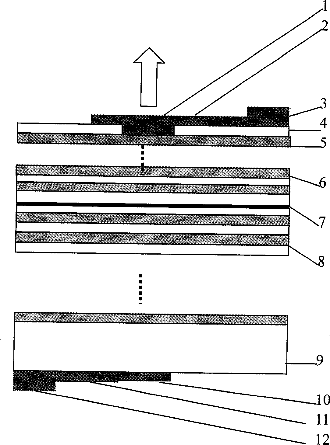
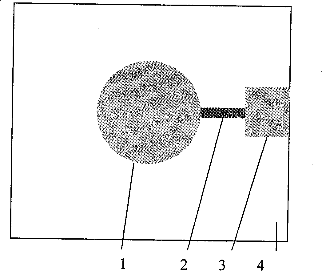
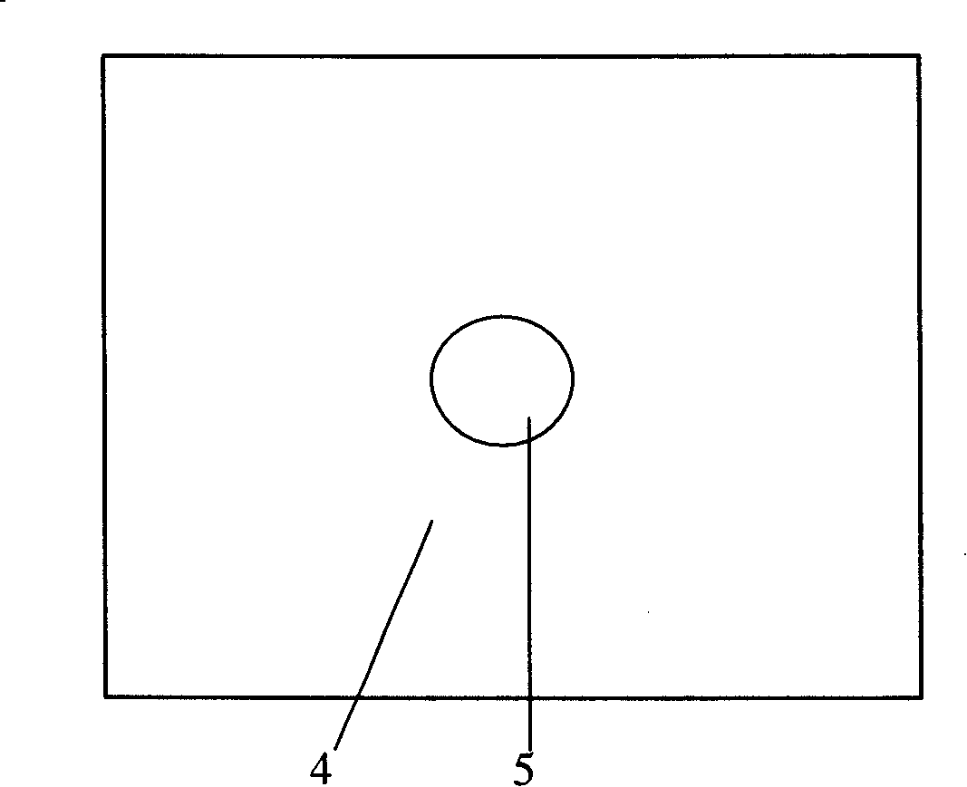
[0040] as the picture shows, figure 1 It is a structural schematic diagram of the product of the present invention; figure 2 The top view of the upper electrode and the top metal film etching area of ​​the vertical cavity surface emitting laser with etched metal film; image 3 Top view of the undoped intrinsically high-resistance region of the etched current aperture, Figure 4 Bottom view of the bottom electrode and the etched area of ​​the metal-plated film of the etched metal film vertical cavity surface emitting laser.

[0041] Among them, 1: the circular metal reflective film etched on the upper surface, with a radius of 4 to 8 microns; 2: the metal film wire etched on the upper surface; 3: the metal film and electrode in contact with the etched electrode on the upper surface; Doped intrinsically high resistance semiconductor material, the radius of the hole is 1-2 mi...


PUM

PropertyMeasurementUnit
Radiusaaaaaaaaaa
Radiusaaaaaaaaaa

Abstract

The invention relates to an etching apex non-doped intrinsic layer asymmetrical metal film vertical cavity surface emitting laser and a preparation method thereof. The invention comprises a Bragg reflector, a high resistive layer, an electrode, a substrate and a quantum well active region. The upper surface is etched with a round metal reflection film, a metal film lead, a contact layer of the metal film and an upper electrode and the upper electrode; the lower surface of the substrate is provided with the round metal reflection film, a lower surface metal film lead and a lower surface electrode. By introducing the non-doped intrinsic layer to etch the current aperture and combining the upper surface with the substrate surface to etch a metal film asymmetrical structure in order to implement the restriction to current and optical field, the invention has the efficacies of the electrode and the reflector of the metal film, simplifies a vertical cavity emitting laser array integration process, reduces the logarithm of distributed Bragg reflector, restricts the diffusion area of the current, improves the photoelectric coupling efficiency of injected current, avoids proton bombardment or respective oxidation process and is beneficial for integration as the intrinsic high-resistive layer and a chip implement the grown in one operation.

Description

technical field [0001] The invention relates to a semiconductor optoelectronic device, in particular to an asymmetric metal film vertical cavity surface-emitting laser for etching the top non-doped intrinsic layer. Background technique [0002] Vertical-cavity surface-emitting lasers (VCSELs) have recently been used in many technologies because of their low threshold, fast response, circular symmetry of emitted light, and easy two-dimensional integration. In dense wavelength division multiplexing, optoelectronic integration, optical fiber High-efficiency light sources such as communications have proved that vertical cavity surface emitting lasers have application value. [0003] The vertical cavity surface emission structure disclosed in Chinese patent CN99253156.X includes the following contents: upper metal electrode, lower metal electrode, quantum well active layer, p+ ohmic contact layer, p-type semiconductor distributed Bragg reflector, n-type semiconductor distributed ...

Claims


Application Information

Patent Timeline
IPC IPC(8): H01S5/183H01S5/187H01S5/34H01S5/028H01S5/00
Inventor 赵红东康志龙何平孙梅韩力英田红丽张效玮
Owner HEBEI UNIV OF TECH
Why Eureka
Try Eureka