Eureka AIR delivers breakthrough ideas for toughest innovation challenges, trusted by R&D personnel around the world.

Method for manufacturing tin solder projection

A technology for solder bumps and a manufacturing method, which is applied in the manufacture of semiconductor/solid-state devices, electrical components, and electrical solid-state devices, etc., can solve problems such as uneven distribution of solder bumps, and achieve the effect of high strength and uniform distribution.

Active Publication Date: 2008-06-25
SEMICON MFG INT (SHANGHAI) CORP +1
View PDF1 Cites 8 Cited by
  • Summary
  • Abstract
  • Description
  • Claims
  • Application Information

AI Technical Summary

Problems solved by technology

[0008] Therefore, the object of the present invention is to provide a kind of manufacturing method of solder bump, to solve the uneven distribution problem of each component in the solder bump that the manufacturing method of existing solder bump forms

Method used


Image

  • Method for manufacturing tin solder projection
  • Method for manufacturing tin solder projection
  • Method for manufacturing tin solder projection

Examples


Embodiment Construction

[0026] In order to make the above objects, features and advantages of the present invention more comprehensible, specific implementations of the present invention will be described in detail below in conjunction with the accompanying drawings.

[0027] Image 6 It is a flow chart of the first embodiment of the manufacturing method of the solder bump of the present invention.

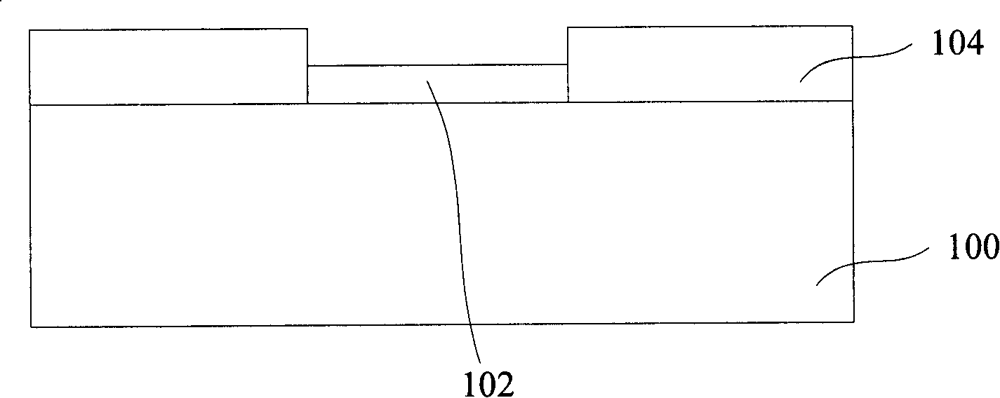
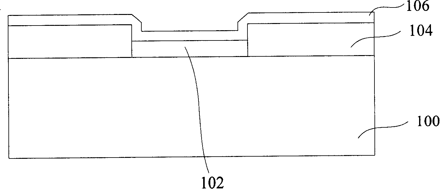
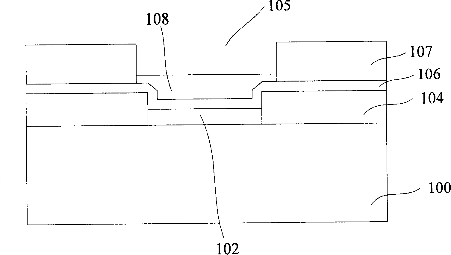
[0028] like Image 6 As shown, firstly, a semiconductor substrate (S100) is provided, the semiconductor substrate is one of monocrystalline silicon, polycrystalline silicon, and amorphous silicon, and the semiconductor substrate has completed the device manufacturing in the front stage and the metal interconnection in the back stage, Lead soldering bumps are formed on the surface of the semiconductor substrate, the soldering wires are aluminum, copper or aluminum-copper alloy, and a protective layer is formed on the surface of the semiconductor substrate other than the soldering wires, and the protectiv...


PUM


Abstract

The invention relates to a manufacturing method of a solder bump. The method comprises the following steps: a semiconductor substrate with a leading wire soldering block is provided; at least one metal layer is formed on the leading wire soldering block; a photoresist layer is formed on the metal layer, and is patterned to form an opening, the opening is positioned the corresponding position above the leading wire soldering block, and the metal layer is exposed from the bottom part of the opening; a solder bump is formed in the opening through using an electroplating method, and the average current density of the electric current in the electroplating method is 3 to 4 ASD; the photoresist layerand the metal layers which are not covered by the solder bump are removed; reflowing is performed to the solder bump. The manufacturing method of the invention enables each component of the formed solder bump to be evenly distributed, the intensity is higher, and the formed solder bump is more favorable for being bonded to a circuit board and other substrates.

Description

technical field [0001] The invention relates to the technical field of semiconductor manufacturing, in particular to a method for manufacturing solder bumps. Background technique [0002] With the development of semiconductor manufacturing technology, the chip size tends to be miniaturized, and the chip density on the circuit board substrate is increasing day by day. Traditional packaging technology is becoming a bottleneck restricting the improvement of circuit performance, prompting the development of chip packaging technology from the original cutting and crimping technology. It is the current flip chip (Flip chip) technology. Flip-chip technology is to form solder bumps (Solder Bump) on the chip's lead pad (Bond Pad) after the chip is manufactured, and directly paste the chip with the solder bump on the printed circuit board ( PCB) or other substrates. This requires the solder bumps on the chip to have good mechanical strength and electrical conductivity. Chinese pate...

Claims


Application Information

Patent Timeline
Patent Type & Authority Applications(China)
IPC IPC(8): H01L21/60
CPCH01L2924/01074H01L24/10H01L24/13H01L2924/01024H01L2924/01082H01L2224/13099H01L2924/01013H01L2924/01022H01L2924/01015H01L2924/014H01L2924/01029H01L2924/01047H01L2924/01006H01L2924/01078H01L2924/01033H01L2924/01079H01L2224/10H01L2224/13H01L2924/00H01L2924/00012
Inventor 王继明李润领孟津梅娜
Owner SEMICON MFG INT (SHANGHAI) CORP
Why Eureka
Eureka Blog
Learn More