A preparation method of nanometer scale W/TiN compound refractory metal bar

A refractory metal, nano-scale technology, applied in semiconductor/solid-state device manufacturing, semiconductor devices, electrical components, etc., can solve problems such as high threshold voltage, and achieve the effect of overcoming excessive threshold voltage

Inactive Publication Date: 2008-07-09
INST OF MICROELECTRONICS CHINESE ACAD OF SCI
View PDF0 Cites 5 Cited by
  • Summary
  • Abstract
  • Description
  • Claims
  • Application Information

AI Technical Summary

Problems solved by technology

However, the surface damage of the sputtered gate electrode to the thin gate oxide layer has always been an unresolved pro

Method used


Image

  • A preparation method of nanometer scale W/TiN compound refractory metal bar
  • A preparation method of nanometer scale W/TiN compound refractory metal bar
  • A preparation method of nanometer scale W/TiN compound refractory metal bar

Examples


Embodiment Construction

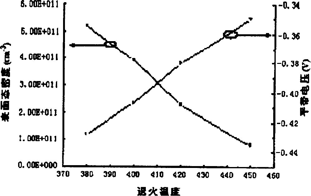
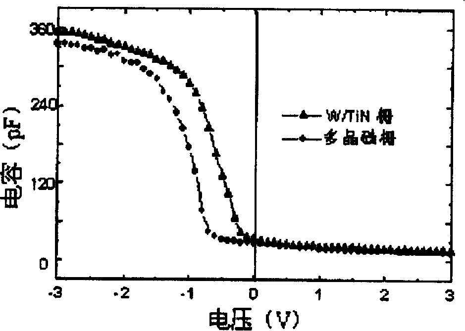
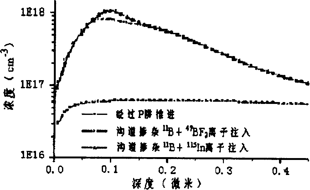
[0028] The following is a CMOS device with a gate length of 90nm (nanometer) W / TiN composite refractory metal gate with excellent performance by applying the method for preparing the W / TiN composite refractory metal gate of the present invention:

[0029] Step 1: Carry out a planarization process after the cobalt silicide in the device source / drain region is formed, then etch the gate groove and float away the replacement gate silicon oxide, and then gate oxidation (a known technology);

[0030] Step 2: Vacuum thermal annealing treatment: background vacuum degree: 8×10 -7 Torr, heat up to 300°C, keep the temperature constant for 10 minutes, then lower the temperature, and wait for the vacuum to return to 8×10 -7 Torr, pre-sputtered TiN 5 min;

[0031] Step 3: Sputter refractory metal TiN, the background vacuum is 8×10 -7 Torr, sputtering power 800 watts, working pressure 5×10 -7 Torr; Ar / N 2 =4 / 1 volume ratio, TiN film thickness is 35nm;

[0032] Step 3: sputtering W film...


PUM


Abstract

The invention relates to a preparation method of a nanometer scale W/TiN composite refractory metal gate, the steps are as follows: a device source/ leakage area cobalt silicide is formed, after that, the flattening process is carried out, a gate groove is corroded, a gate silicon oxide is bleached and replaced, then the gate is oxidized again; the vacuum thermal annealing processing is carried out; a refractory metal TiN is sputtered, the thickness is 25 to 45nm; a W thin film is sputtered, the thickness is 90 to 110nm; the acetone and the anhydrous ethanol are used for ultrasonic cleaning, the deionized water is used for flushing, and the drying is carried out in hot N2; the W/TiN T-shaped gate is done with the lithography; the W/TiN T-shaped gate is etched by reaction ions, the etching gas is C12 and SF6; a chemical vapor deposition SiO2 is strengthened by a plasma, the thickness of SiO2 is 500 to 700nm; a contact hole is formed; and the metallizing annealing is carried out. The invention solves a series of serious problems of excessive high gate resistance, serious boron penetration of a PMOS device, polysilicon gate depletion, incompatibility with a high k gate dielectric and so on which exist in the conventional polysilicon gate, so the invention can obtain excellent device properties.

Description

technical field [0001] The invention belongs to the technical field of nano-scale CMOS devices and semiconductor integration, and in particular relates to a preparation method for W / TiN composite refractory metal gates used in the manufacture of nano-scale CMOS devices. Background technique [0002] When the gate length of polysilicon gate MOSFET"s shrinks to the nanometer scale, conventional polysilicon gates are thermally stable due to excessive gate resistance, severe boron penetration effect of PMOS devices, polysilicon gate depletion effect, and incompatibility with high-K gate dielectrics. The performance is not good, there are a series of serious problems such as the Fermi pinning effect, which has become a bottleneck for further improving the performance of CMOS devices. Using refractory metals instead of traditional doped polysilicon as the gate electrode of MOSFET's can satisfactorily solve the above problems, and there is hope Applied for the next generation of in...

Claims


Application Information

Patent Timeline
IPC IPC(8): H01L21/28H01L21/336
Inventor 徐秋霞李瑞钊
Owner INST OF MICROELECTRONICS CHINESE ACAD OF SCI
Why Eureka
Try Eureka