

Laser modeling method for semiconductor material micro-nano multi-scale function surface
A surface micromodeling and semiconductor technology, which is applied in semiconductor/solid-state device manufacturing, laser welding equipment, nanostructure manufacturing, etc., can solve the problems of high cost, difficult operation, low efficiency, etc., and achieve low cost, high preparation efficiency, and easy operation. simple effect
- Summary
- Abstract
- Description
- Claims
- Application Information
AI Technical Summary
Problems solved by technology
Method used
Image

Examples
Embodiment Construction
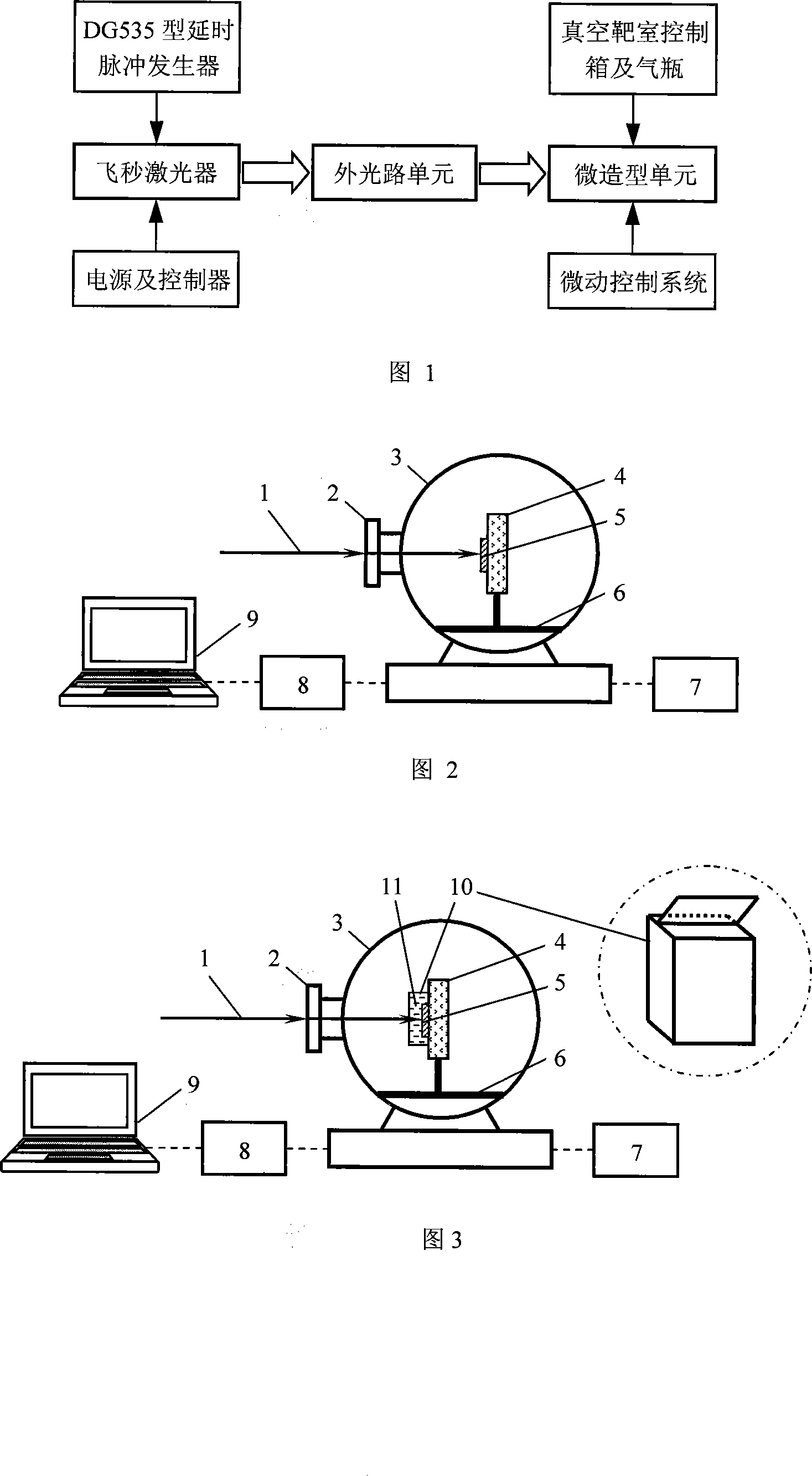
[0029]Figure 1 is a block diagram of a micro-nano multi-scale functional surface laser micro-modeling system. The laser micro-modeling system mainly includes three parts: a femtosecond laser, an external optical path unit and a micro-modeling unit. The DG535 delay pulse generator connected to the femtosecond laser is used to control the number of laser action pulses, while the power supply and controller are used to control the output of the laser and adjust the laser energy. The vacuum target chamber control box and the gas cylinder connected with the micro-modeling unit are used to set the vacuum degree and control the background gas filling and air pressure respectively. The micro-motion control system is composed of a three-dimensional micro-motion axis, a stepping motor, and a computer connected in sequence , used to scan the surface of the sample in multiple directions.
[0030] Figure 2 is a schematic diagram of the micro-modeling unit when the sample is in a vacuum-fi...
PUM
| Property | Measurement | Unit |
|---|---|---|
| diameter | aaaaa | aaaaa |
Abstract
Description
Claims
Application Information