Gas treatment apparatus

A technology of gas treatment and gas injection, which is applied in the fields of electrical components, gaseous chemical plating, semiconductor/solid-state device manufacturing, etc. Occurrence of film formation defects, suppression reduction, and effects of variation

Active Publication Date: 2008-07-16
TOKYO ELECTRON LTD
View PDF1 Cites 8 Cited by
  • Summary
  • Abstract
  • Description
  • Claims
  • Application Information

AI Technical Summary

Problems solved by technology

[0007] However, as described above, when a flat gas diffusion space is provided in the shower head, since this space prevents transfer (radiation) to the back side, it is heated by radiant heat from the mounting table for heating the semiconductor wafer. The film causes the temperature rise of the nozzle
[0008] Especially in MOCVD, since the thermal decomposition of the raw material gas is used, when the temperature of the shower head rises and the temperature exceeds the thermal decomposition temperature of the raw material gas, an undesirable thermal decomposition reaction occurs inside the shower head, in the piping in front of the shower head, etc., The concentration of the raw material gas supplied to the semiconductor wafer is lowered, or the reflectance of the shower head is lowered due to the decomposition product of the raw material gas attached to the surface of the shower head, and the temperature of the semiconductor wafer is lowered, resulting in a poor film formation.
[0009] Moreover, when the temperature of the shower head rises over time as described above, it becomes the cause of large variations in film quality and film composition, and the above-mentioned decomposition products are peeled off from the surface of the shower head to fly and fall on the semiconductor wafer as foreign matter, which also causes Causes of poor film formation

Method used


Image

  • Gas treatment apparatus
  • Gas treatment apparatus
  • Gas treatment apparatus

Examples


Embodiment Construction

[0028] Embodiments of the present invention will be specifically described below with reference to the drawings.

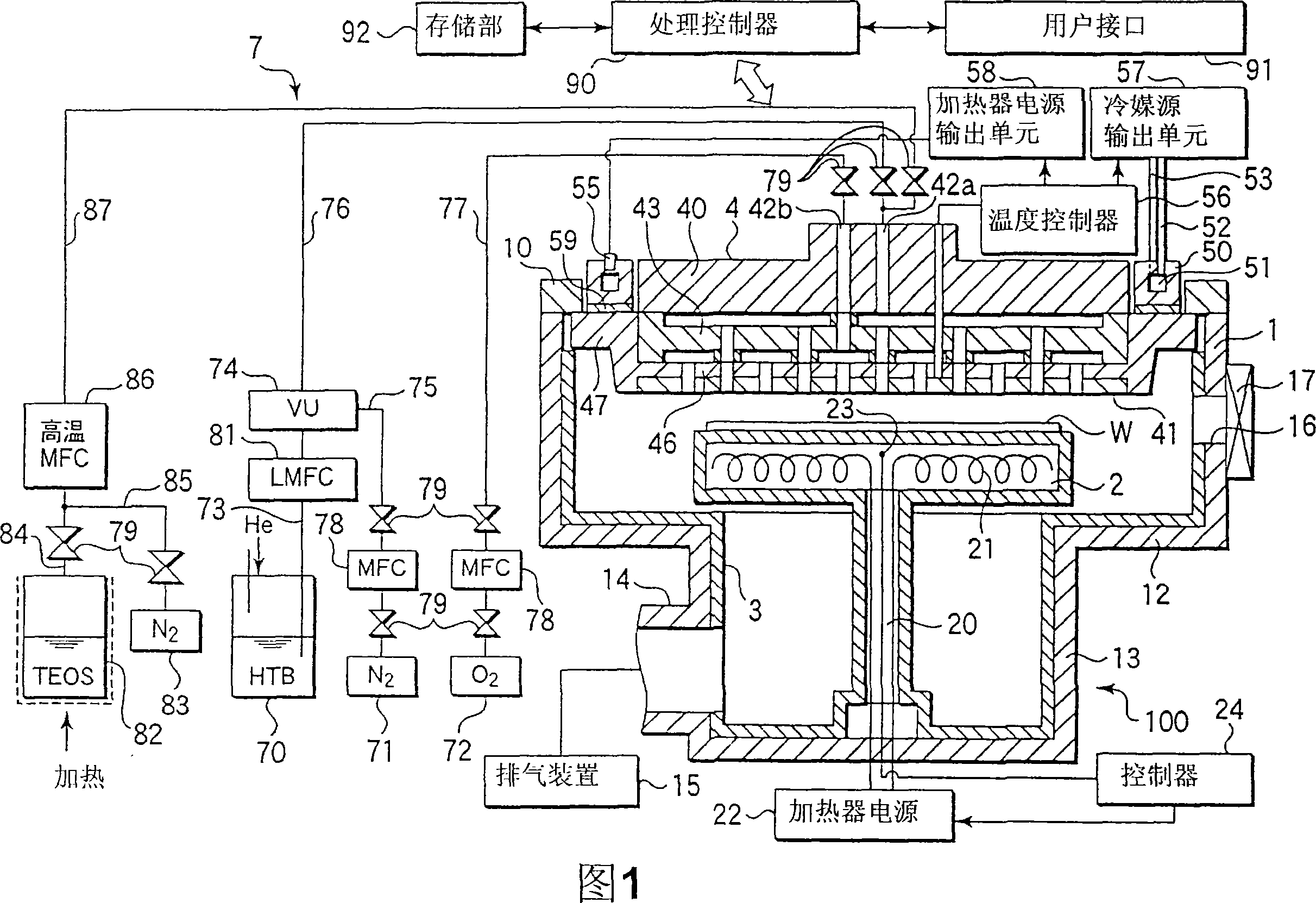
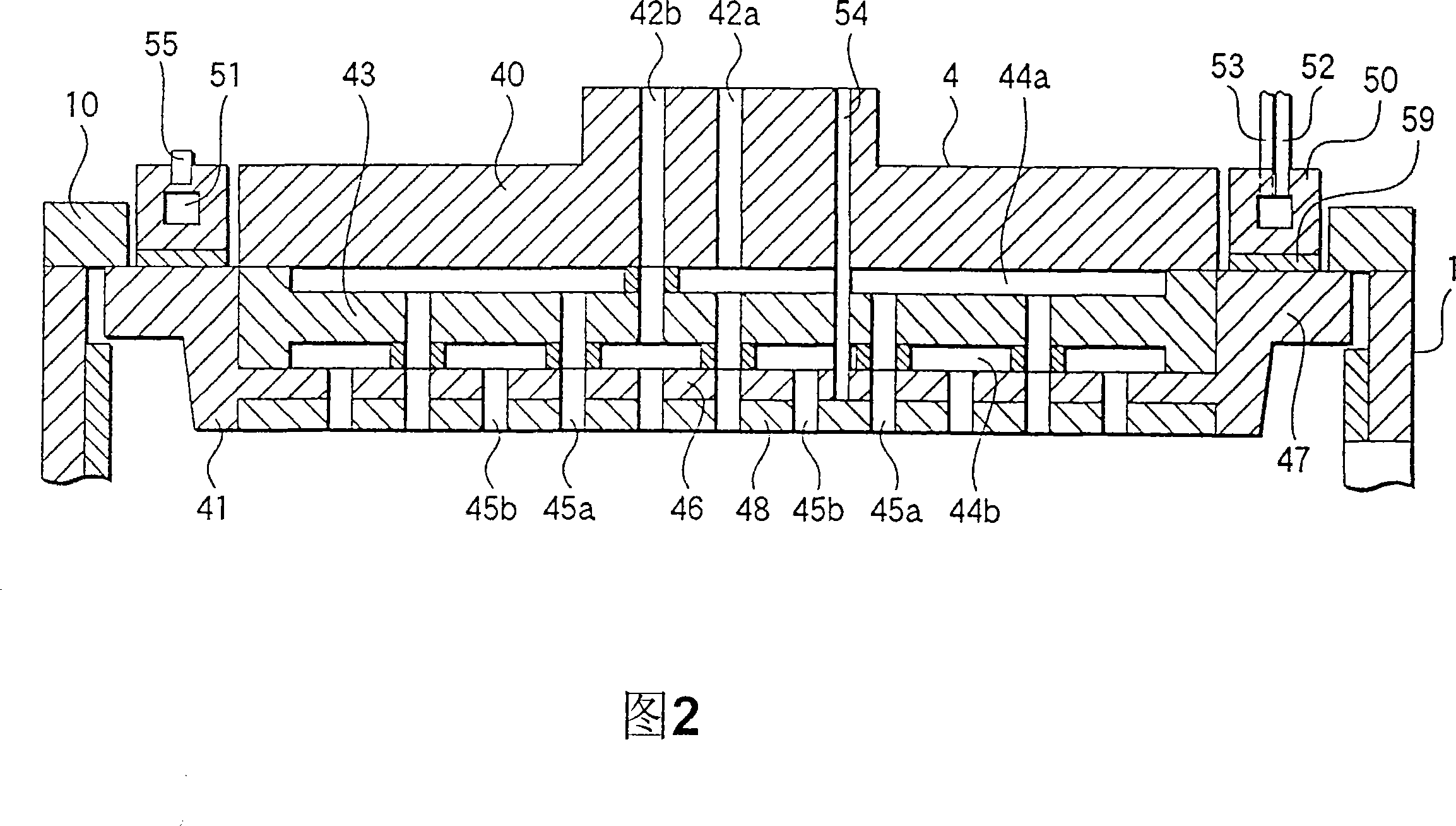
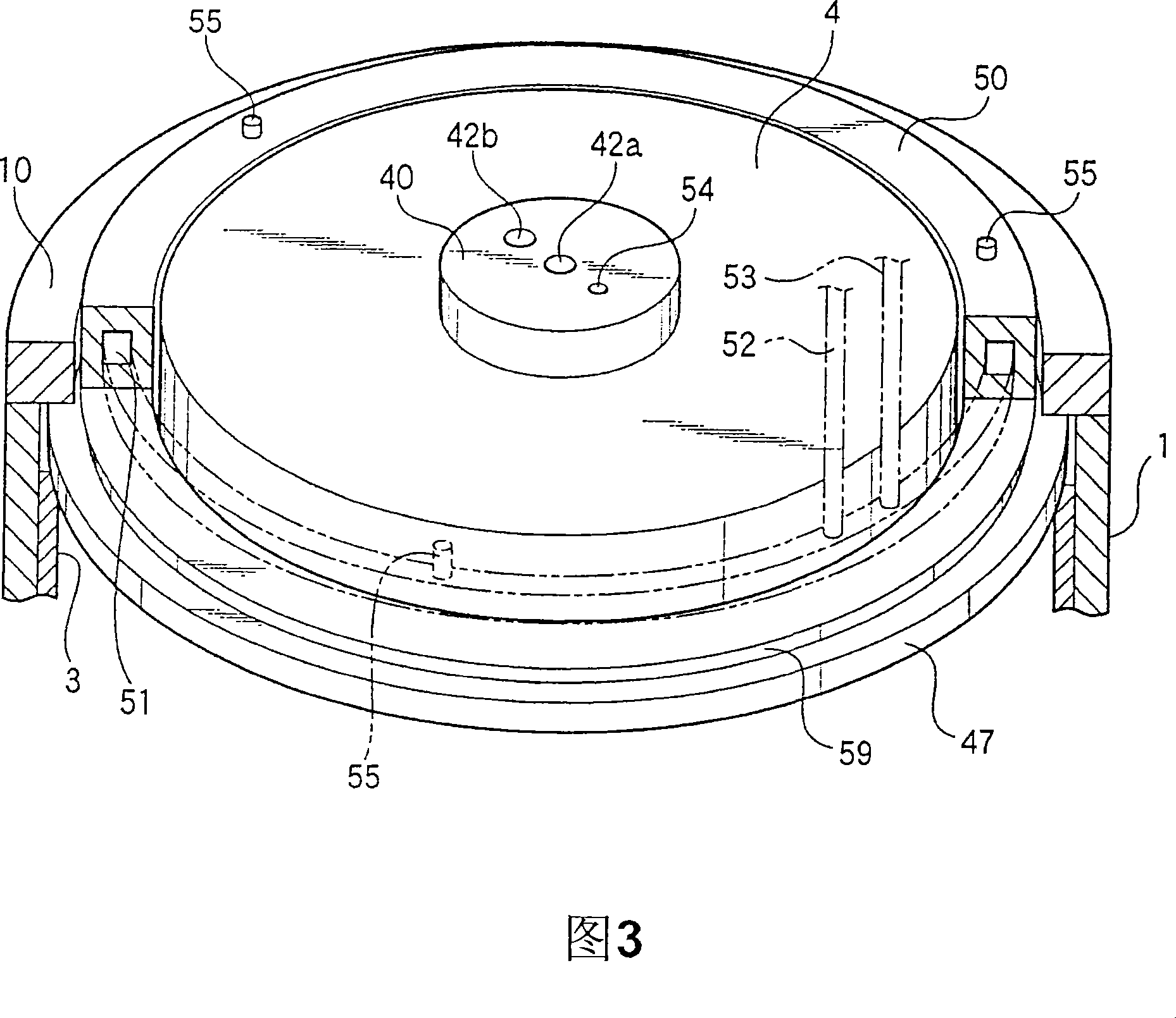
[0029] 1 is a cross-sectional view showing a film forming apparatus according to an embodiment of the gas processing apparatus of the present invention, FIG. 2 is a cross-sectional view showing a main part of a chamber and a shower head constituting the film forming apparatus, and FIG. 3 is a cross-sectional view showing a chamber and a shower head. A cutaway perspective view of the main part of the nozzle.

[0030]This film forming apparatus 100 has an airtight substantially cylindrical chamber 1 as a processing container, in which a mounting table 2 for horizontally supporting a Si substrate (wafer) W as an object to be processed is arranged so as to pass through the center thereof. It is arranged in a state supported by the lower cylindrical support member 20 . The mounting table 2 is made of ceramics such as AlN. In addition, a heater 21 is embedded in the m...


PUM


Abstract

The present invention relates to gas treatment plants. The film-forming device (100) includes: a chamber (1) for accommodating wafers; a mounting table arranged in the chamber (1) for mounting the wafers; a mounting table arranged at a position opposite to the mounting table, facing into the chamber (1) A spray head (4) for spraying processing gas; and an exhaust mechanism for exhausting the inside of the chamber (1). The shower head (4) includes: a central portion (46) formed with a large number of gas ejection holes (45a, 45b) for ejecting processing gases; a gas ejection hole (45a) that is located on the outer peripheral side of the central portion (46) , 45b), the film forming device (100) further includes a heat dissipation mechanism for dissipating heat from the spray head (4) from the entire circumference of the outer periphery (47) to the atmosphere side.

Description

technical field [0001] The present invention relates to a gas processing apparatus for gas processing a substrate to be processed using a processing gas. Background technique [0002] In recent years, based on the requirements of high integration and high speed of LSI, the design rules of semiconductor elements constituting LSI have become increasingly finer. At the same time, in CMOS devices, SiO 2 EOT (Equivalent Oxide Thickness: Equivalent Oxide Thickness) of film thickness in terms of capacitance is a value of about 1.5 nm or less. As a material for realizing such a thin insulating film without increasing gate leakage current, a high dielectric constant material, that is, a so-called High-k material, is attracting attention. [0003] In the case of using a high dielectric constant material as the gate insulating film, it must be thermodynamically stable without interdiffusion with the silicon substrate. From this point of view, oxides of hafnium, zirconium, or lanthanum...

Claims


Application Information

Patent Timeline
Patent Type & Authority Applications(China)
IPC IPC(8): H01L21/31C23C16/455
CPCC23C16/45565H01L21/67109H01L21/31645C23C16/45574H01L21/31608C23C16/401H01L21/02181H01L21/02164H01L21/31C23C16/4412
Inventor 松岛范昭高桥毅
Owner TOKYO ELECTRON LTD
Why Eureka
Try Eureka