Solder tray local tin plating method on circuit board
A circuit substrate and local plating technology, which is applied in the direction of assembling printed circuits with electrical components, can solve problems such as increased processing costs, low welding quality, and difficulties, and achieve the effects of strengthening mechanized operations, improving production efficiency, and reducing production costs
- Summary
- Abstract
- Description
- Claims
- Application Information
AI Technical Summary
Problems solved by technology
Method used
Image
Examples
Embodiment Construction
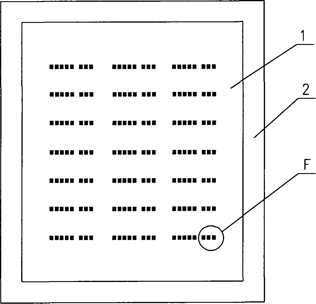
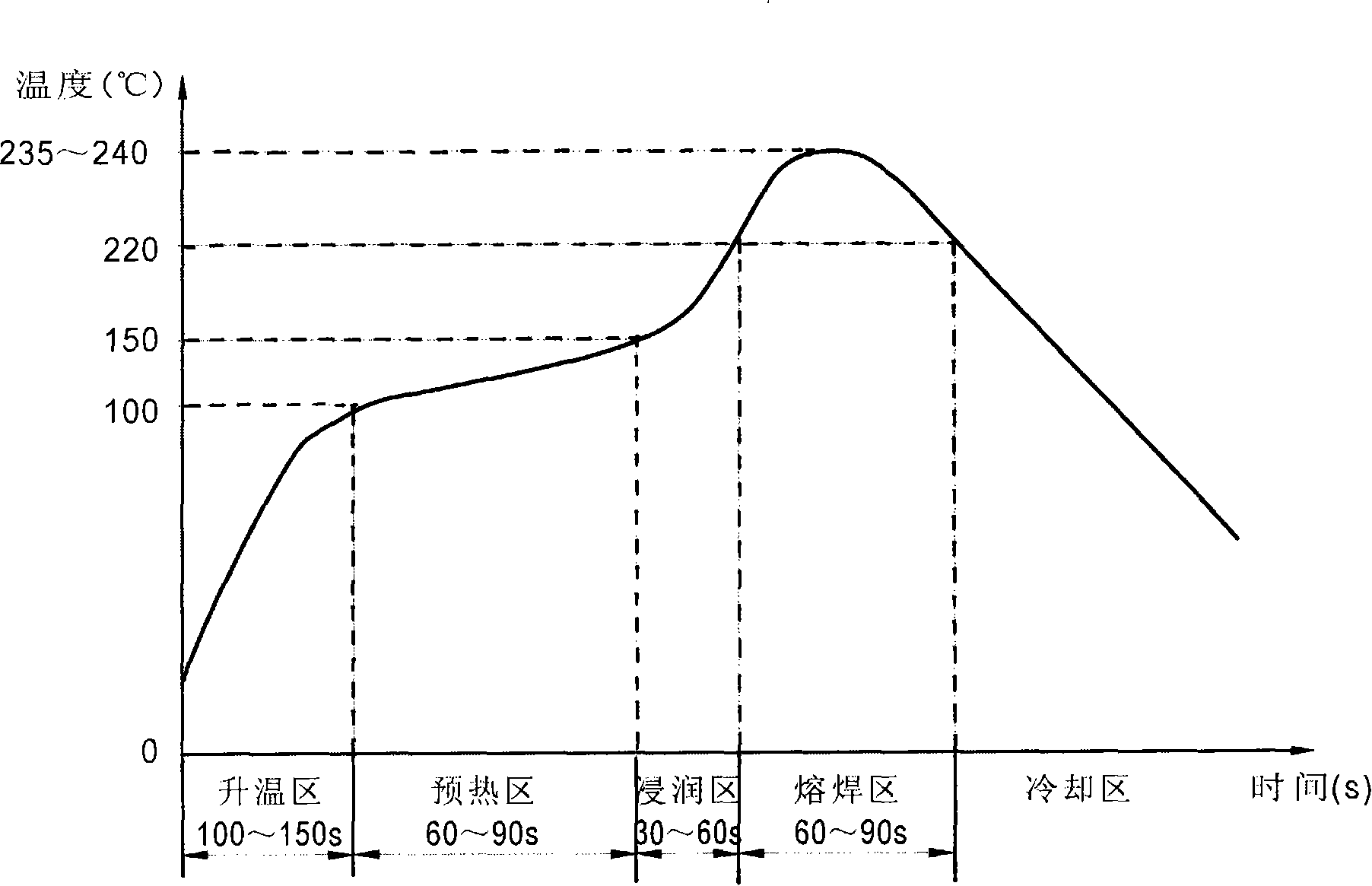
[0026] A local tinning method for pads on a circuit substrate of the present invention comprises the following steps: brushing the lead-free tin paste into the spot welding pads of the circuit substrate through a steel mesh; The welding machine sets five areas of working parameters to form a liquid tin coating that fills the entire spot welding pad. After the circuit substrate is cooled, a solid tin coating is formed in the spot welding pad.
[0027] The above-mentioned circuit substrate is a copper-clad lead-free tin printed circuit board made of FR-4; the pad refers to the exposed metal surface on the substrate where the components are designed to be placed, that is, the tin-plated surface, and the spot welding pad refers to For the position of the pad that needs to be processed by spot welding, the composition of the above-mentioned lead-free solder paste is creamy solder with Sn96.5%, Ag3%, and Cu0.5%.
[0028] Such as figure 1 , figure 2 As shown, the above-mentioned s...
PUM
 Abstract
Description
Claims
Application Information


