A p type conductive transparent nickel-doped CuO film and its making method

A conductive transparent, copper oxide technology, applied in the direction of circuits, electrical components, semiconductor devices, etc., can solve the problem of low energy conversion efficiency and achieve the effect of high conductivity

Inactive Publication Date: 2008-09-10
FUDAN UNIV
View PDF0 Cites 2 Cited by
  • Summary
  • Abstract
  • Description
  • Claims
  • Application Information

AI Technical Summary

Problems solved by technology

Solar photovoltaic power generation is receiving unprecedented attention in v...

Method used


Image

  • A p type conductive transparent nickel-doped CuO film and its making method
  • A p type conductive transparent nickel-doped CuO film and its making method
  • A p type conductive transparent nickel-doped CuO film and its making method

Examples


Embodiment 1

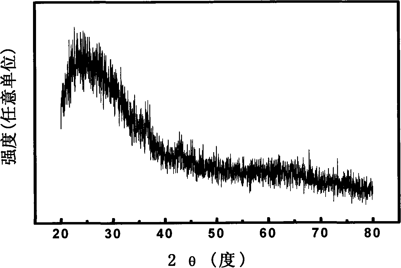
[0021] Example 1, prepare Cu with a certain chemical dosage ratio according to the traditional ceramic target preparation method 0.95 Ni 0.05 O circular target with a target diameter of 23.4 mm. The substrate is a common glass slide, which is ultrasonically cleaned with deionized water, acetone and alcohol for 20 minutes each. The distance between the target surface and the quartz tube was fixed at 4 mm, and the inner diameter of the quartz tube was 2 mm.

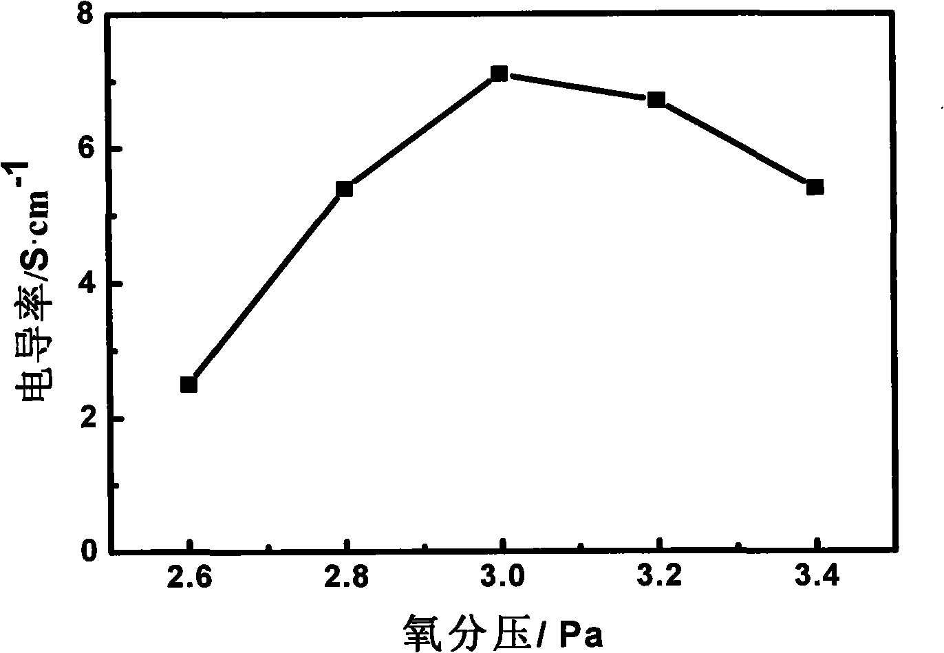
[0022] The background pressure of the vacuum chamber before film deposition was 2.0×10 -4 Pa, the substrate temperature is 30°C, set O 2 For the working air pressure, the mass flowmeter of Bronkhorst Company is used to control its flow, so that the working air pressure is 3.0Pa, and the temperature of the substrate is measured by the Eliwell EWTQ 915 thermocouple. -18.0KV and 4.5mA, the frequency of the pulsed electron beam is 2.0Hz, and the film is prepared on a common glass plate. The film deposition time is 20 minut...

Embodiment 2

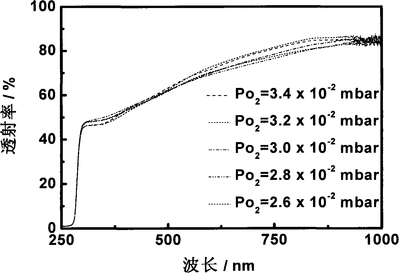
[0023] Embodiment 2, the same method as embodiment 1 prepares Cu 0.95 Ni 0.05 O ceramic target, Cu was prepared under the following conditions 0.95 Ni 0.05 O film: the background pressure of the vacuum chamber before film deposition is 2.0×10 -4 Pa, the substrate temperature is 30°C, and the set working pressure is O 2 It is 3.0Pa, the operating voltage and current are -17.0KV and 4.5mA respectively, and the frequency of the pulsed electron beam is 2.0Hz. The film deposition time is 20 minutes, the film thickness is 80nm, and the conductivity is 5.9S cm -1 , the average transmittance in the visible region is higher than 65%.

[0024] A Kosaka ET3000 surface profiler was used to measure the film thickness, a BD-90 four-probe instrument was used to measure the film sheet resistance and target resistivity, and a Shimadzu UV2450 UV / Visible spectrophotometer was used to measure the film transmission spectrum. The conductive properties of the target and film were qualitatively...


PUM

PropertyMeasurementUnit
The inside diameter ofaaaaaaaaaa
Thicknessaaaaaaaaaa
Conductivityaaaaaaaaaa

Abstract

The invention pertains to the technical field of transparent conductive oxide films, more particularly relates to a P-type conductive transparent cooper oxide film doping with nickel and a preparation method thereof. Common glass is taken as a base plate o the P-type conductive transparent cooper oxide film doped with nickel and cooper oxide film doped with nickel, (Cu1-xNixO) ceramic target is utilized, under the condition that the temperature of the base plate is room temperature, the P-type conductive transparent Cu1-xNixO film with a non crystalline structure is obtained by pulsed plasma deposition (PPD) technique under the condition of proper oxygen pressure, pulsed current and pulsed voltage. The film prepared by the method has high electric conductivity and good current-illumination characteristics such as high transmissivity within the range of visible light, etc. The P-type conductive transparent oxide film obtained by the method of the invention has better application prospect in the fields of transparent electronics and novel photoelectric devices.

Description

technical field [0001] The invention belongs to the technical field of transparent conductive films, and in particular relates to a p-type conductive transparent oxide film material and a preparation method thereof. Background technique [0002] Transparent conductive oxide (TCO) thin film is an oxide semiconductor material, which is widely used in flat panel display, solar cell and other fields due to its unique combination of transparency and conductivity. According to reports, in 2004, the market transactions related to flat panel display were nearly 25 billion US dollars, which shows the importance of transparent conductors. TCO thin films can be divided into n-type and p-type according to their conductivity. n-type TCO materials such as In 2 o 3 :Sn(ITO) and SnO 2 :F (FTO) as a transparent electrode, its photoelectric properties have reached a good level. Although the research on the corresponding p-type TCO materials has been carried out and achieved certain resul...

Claims


Application Information

Patent Timeline
IPC IPC(8): H01L31/0224H01L31/18C23C14/08C23C14/34C23C14/54
CPCY02P70/50
Inventor 张群施展杨铭王颖华
Owner FUDAN UNIV
Why Eureka
Try Eureka