Method for making CIS film based on neutral pH condition double potential step electrodeposit

An electrodeposition, bipotential technology, applied in circuits, electrical components, semiconductor devices, etc., can solve problems such as limitations and difficulty in finding deposition potentials

Inactive Publication Date: 2008-09-10
TIANJIN UNIV
View PDF0 Cites 12 Cited by
  • Summary
  • Abstract
  • Description
  • Claims
  • Application Information

AI Technical Summary

Problems solved by technology

Therefore, under the existing acidic or alkaline conditions, CuInSe 2 The preparation of thin films is still limited in these application technology occasions, seeking to prepare CuInSe under near-neutral and mild conditions 2 Thin films have important application value and have clear significance for the development of low-cost thin-film solar cells
[0004] For CuInSe under mi...

Method used


Image

  • Method for making CIS film based on neutral pH condition double potential step electrodeposit
  • Method for making CIS film based on neutral pH condition double potential step electrodeposit
  • Method for making CIS film based on neutral pH condition double potential step electrodeposit

Examples


Embodiment Construction

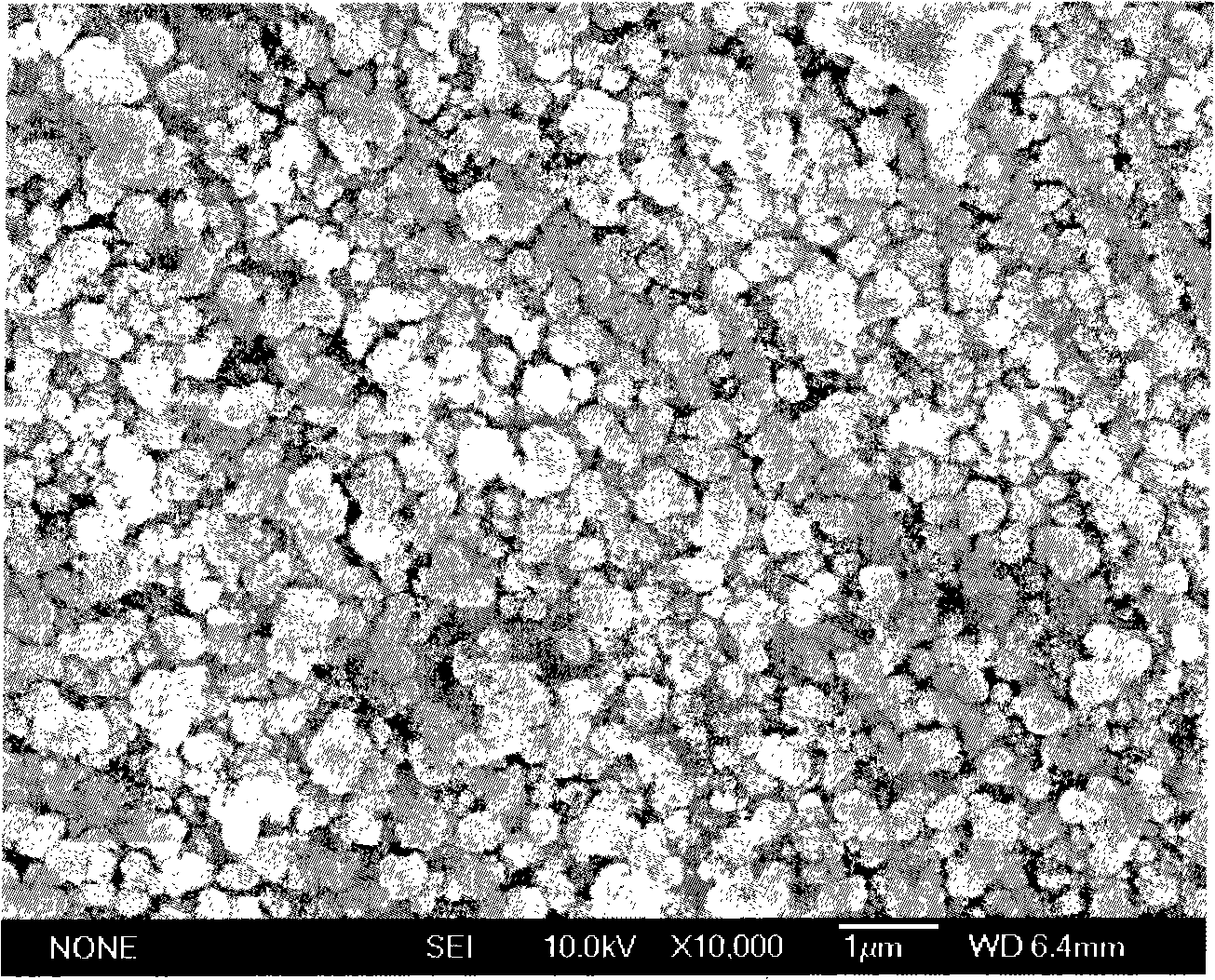
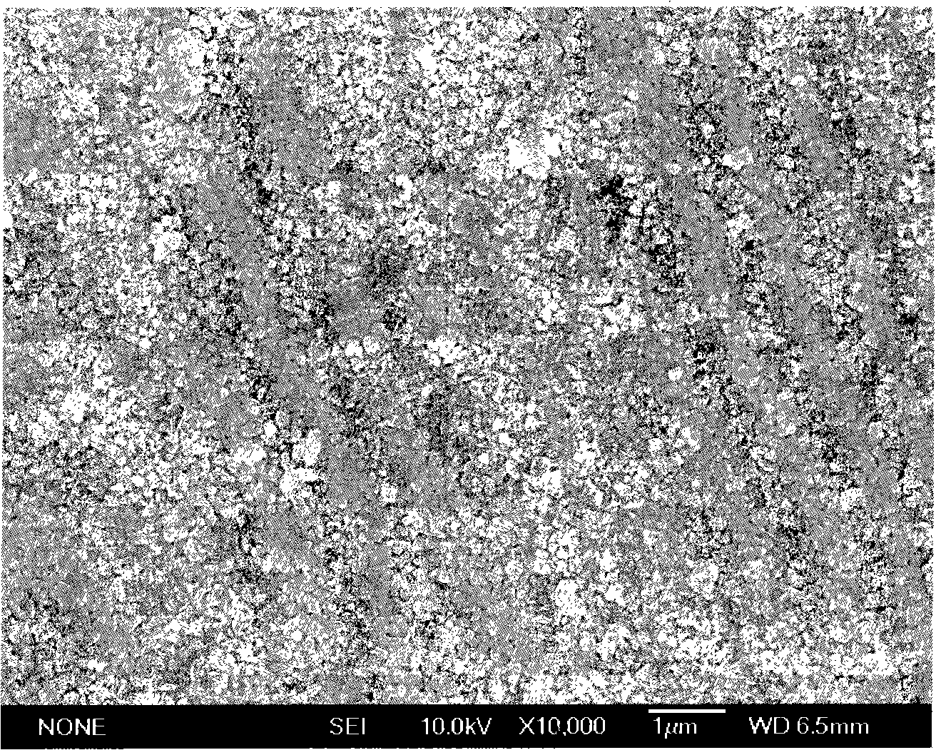
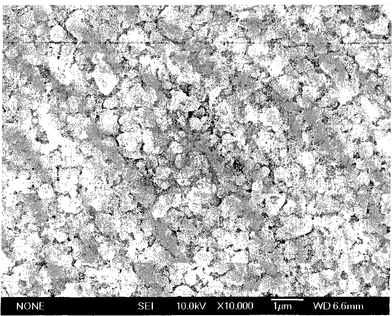
[0017] The embodiment of the present invention uses chemically pure raw materials. The composition of the electrodeposition solution of the specific embodiment is shown in Table 1, and the parameters of the bipotential step deposition are shown in Table 2.

[0018] Table 1

[0019]

No.

CuCl 2 (mM)

InCl 3 (mM)

SeO 2 (mM)

C 6 h 5 Na 3 o 7- 2H 2 O(mM)

pH

1

2.0

1.0

3.0

15

6.5

2

1.2

0.8

2.0

15

6.5

3

1.0

0.6

1.6

14

7.0

4

1.0

0.6

1.6

14

7.0

5

1.0

2.0

3.0

15

6.5

6

1.0

0.6

1.6

14

7.0

[0020] Table 2

[0021]

No.

Step potential point 1 / continuous

Time (mV / s)

Step potential point 2 / continuous

Time (mV / s)

Cycles

...


PUM


Abstract

The invention discloses a method for preparing a copper indium diselenide film by bipotential phase step electrodeposition under neutral pH value, which comprises the steps that: (1) electrodeposition solution is prepared and pH value thereof is 6.5-7.0; (2) a way of bipotential phase step is adopted for plating a film; (3) the film is evaporated in air at room temperature; (4) the film goes through thermal treatment in argon atmosphere at 400 DEG C for 0.5 hour and a CuInSe2 film with copper pyrite structure being obtained. The method adopts the bipotential phase step electrodeposition method for the first time, takes CuCl2question mark 2H2O, InCl3question mark 4H2O and SeO2 as raw materials and CirNa as a complexing agent, which solves the problem of the deposition of the CuInSe2 film on matrixes which have poor acid and alkali resistance and are easily corrosive such as ZnO, etc. The method is an important part of a film solar battery and is used for solar batteries and a plurality of light sensors, etc.

Description

technical field [0001] The present invention relates to the preparation of photovoltaic semiconductor thin films by electrodeposition methods, in particular to the preparation of copper indium selenium (CuInSe) by double potential step electrodeposition. 2 ) film method. technical background [0002] Copper Indium Tin (CuInSe 2 ) is a direct band gap semiconductor material with a band gap of 1.04eV. Due to its high photoelectric conversion efficiency (18%) and light absorption coefficient (α>10 -5 cm -1 ), has strong radiation resistance, and is one of the photovoltaic semiconductor materials with the best absorption performance known so far. With the development of solar cell industry, copper indium tin (CuInSe 2 ) research has also received more and more attention, and is considered to be an important part of thin-film solar cells. At present, it has been used in solar cells and some photosensitive elements at home and abroad. [0003] Copper indium tin (CuInSe) f...

Claims


Application Information

Patent Timeline
IPC IPC(8): H01L31/18
CPCY02P70/50
Inventor 靳正国李成杰杨靖霞王文静
Owner TIANJIN UNIV
Why Eureka
Try Eureka