Press welding method for semiconductor extension film

A technology of epitaxial wafers and semiconductors, applied in semiconductor devices, electrical components, circuits, etc., can solve the problems of slow heating rate, long cooling time, and affecting ohmic contact, and achieve fast heating rate, fast heating rate and cooling rate, and improved The effect of production rate

Inactive Publication Date: 2008-09-17
LATTICE POWER (JIANGXI) CORP
View PDF0 Cites 5 Cited by
  • Summary
  • Abstract
  • Description
  • Claims
  • Application Information

AI Technical Summary

Problems solved by technology

When the InGaAlN film grown on the original substrate is made into a light-emitting device, there will be the following disadvantages: low utilization rate of the light-emitting material, poor heat dissipation, and the P-type transparent conductive layer has a certain absorption effect on light, thus affecting the photoelectricity of the device. There is a certain impact on performance
However, the metal has a large specific heat capacity, so its heating rate is slow and the heating time is long, which makes the bonding metal easily diffuse to the surface of GaN and damage the ohmic contact performance of the epitaxial wafer
For cooling, if gas cooling or liquid cooling is used, the metal heater will generate a large internal stress and cause deformation; if gas cooling or liquid cooling is not used, the cooling time will be very long, which will not only affect the ohmic contact, but also affect production. efficiency
Repeated heating of the metal heater will cause thermal fatigue, which will deform the heater and cause cracks

Method used


Image

  • Press welding method for semiconductor extension film
  • Press welding method for semiconductor extension film
  • Press welding method for semiconductor extension film

Examples


Embodiment 1

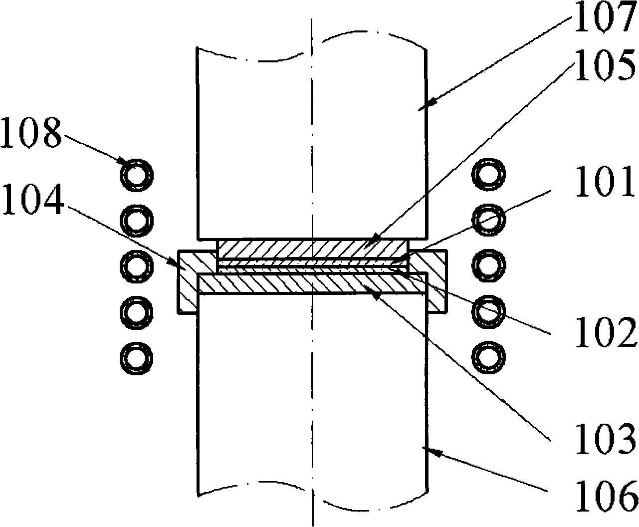
[0023] Construction embodiment one, refer to figure 1 shown. First, an ohmic contact layer and a metal bonding layer (that is, the bonding metal to be bonded) are prepared on the InGaAlN epitaxial wafer 101 , and the ohmic contact layer and the metal bonding layer are prepared on the substrate 102 . If the substrate 102 is metallic, it is not necessary to prepare an ohmic contact layer on the substrate 102 . Of course, it is also possible that only the bonding surface of the epitaxial wafer or one of the substrates has a bonding metal layer. The clamping device that applies pressure to the epitaxial wafer 101 and the substrate 102 includes a pressure applying member 107 and a pressure receiving member 106 . The pressure source of the pressure applying member 107 may be the pressure transmitted by air pressure or the pressure transmitted by hydraulic pressure. In order to obtain high-quality soldering products, the connection between the pressure applying member 107 and the ...

Embodiment 2

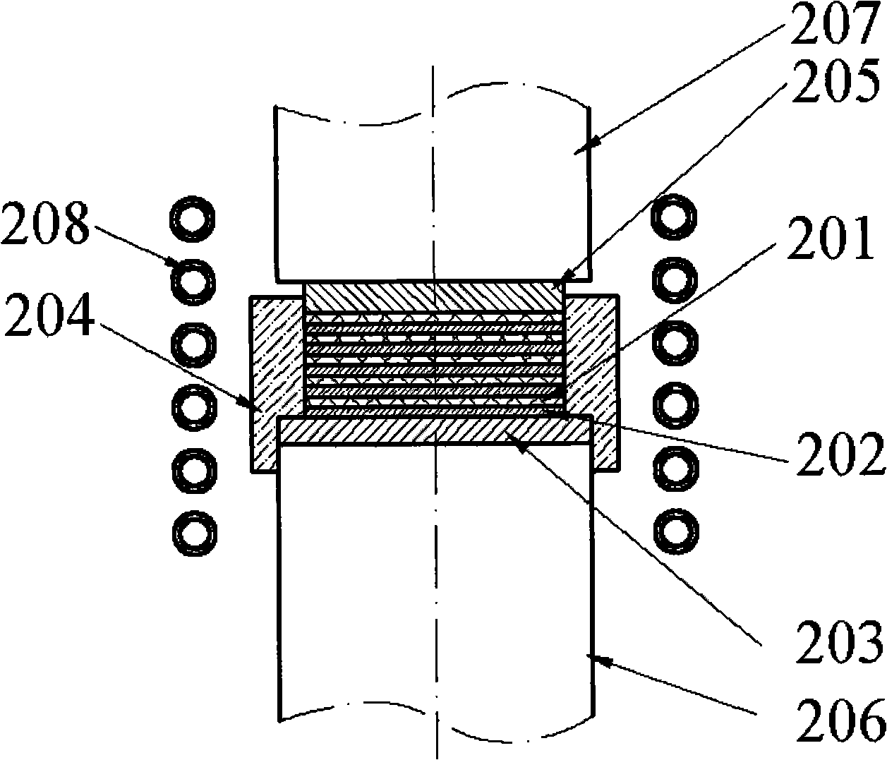
[0035] Construction embodiment two, such as figure 2 shown. An epitaxial wafer and a substrate form a pair of welded bodies. The structure of this embodiment is an improved structure on the structure of the first embodiment in order to improve production efficiency. It can weld multiple welded bodies at one time. This structure needs to lengthen the positioning ring 204 and thicken the upper positioning disc 205 and the lower positioning disc 203 . The structure of the pressing member 207, the pressure receiving member 206 and the electromagnetic coil 208 is the same as that of the first embodiment. The welding body composed of the epitaxial wafer 201 and the substrate 202 can be stacked and placed on the workbench for welding. Because the induced current of the electromagnetic coil heats the epitaxial wafer and the substrate, all the epitaxial wafers and the substrate have a consistent heating rate. The effect is as good as the single welding effect of the embodiment, so t...


PUM


Abstract

The invention discloses a semiconductor epitaxial wafer press-welding method, the method does not need to heat the press-welding method through the way of thermal resistance heating, thus preventing the press-welding method in the way of thermal resistance heating from effecting ohmic contact performance of the epitaxial wafer because of thermal diffusion. The method avoids farthest deterioration of quality of epitaxial wafer caused by the way of thermal resistance heating. The invention comprises the following steps: location steps: placing welding epitaxial wafer and substrate on a worktable of folder device, causing welded surface of the epitaxial wafer and the substrate location-docking through a location device; electromagnetic-welding steps: connecting electromagnetic coil, imposing folder pressure on the epitaxial wafer and the substrate through the folder device of welding body, heating the press-welding method of the epitaxial wafer or the substrate through electromagnetic wave which is sent out by electromagnetic coil, thus causing the epitaxial wafer and the substrate press-welding together. The invention can increase the production rate because of fast heating rate and cooling rate obviously.

Description

technical field [0001] The invention relates to a pressure welding method for semiconductor epitaxial wafers. Background technique [0002] InGaAlN semiconductor light-emitting devices are widely used in full-color large-screen displays, traffic lights, backlights, solid-state lighting, etc. Commonly used substrate materials for InGaAlN semiconductor luminescent materials are sapphire, silicon carbide and silicon. When the InGaAlN film grown on the original substrate is made into a light-emitting device, there will be the following disadvantages: low utilization rate of the light-emitting material, poor heat dissipation, and the P-type transparent conductive layer has a certain absorption effect on light, thus affecting the photoelectricity of the device. There is a certain impact on performance. Using a combination of epitaxial wafer bonding (wafer bonding) and wet lift-off or laser lift-off, the InGaAlN film grown on the original substrate is transferred to a new substra...

Claims


Application Information

Patent Timeline
IPC IPC(8): H01L33/00
Inventor 熊传兵江风益王立王古平章少华
Owner LATTICE POWER (JIANGXI) CORP
Why Eureka
Try Eureka