Device for testing leadless solder welding spot crystal crack

A crystal crack, lead-free solder technology, used in optical testing flaws/defects, metal processing, etc., to ensure reliability, small size, and good reproducibility

Inactive Publication Date: 2011-05-11
BEIJING UNIV OF TECH
View PDF1 Cites 0 Cited by
  • Summary
  • Abstract
  • Description
  • Claims
  • Application Information

AI Technical Summary

Problems solved by technology

[0004]Because in the electronic packaging industry, the size of solder joints is getting smaller and smaller, the crystallization cracks on the surface cannot be found macroscopically, and are easily overlooked, resulting in the failure of solder joints Decrease in static strength and fatigue strength; and it is also difficult to choose lead-free solder
The crystallization cracks on the surface of solder alloys that deviate from the eutectic point have been confirmed in experiments, and their influence on the static strength and fatigue strength of solder joints cannot be ignored, but there is no related crystallization crack heat of lead-free solder. Crack tendency evaluation method and related devices

Method used


Image

  • Device for testing leadless solder welding spot crystal crack
  • Device for testing leadless solder welding spot crystal crack
  • Device for testing leadless solder welding spot crystal crack

Examples


Embodiment 1

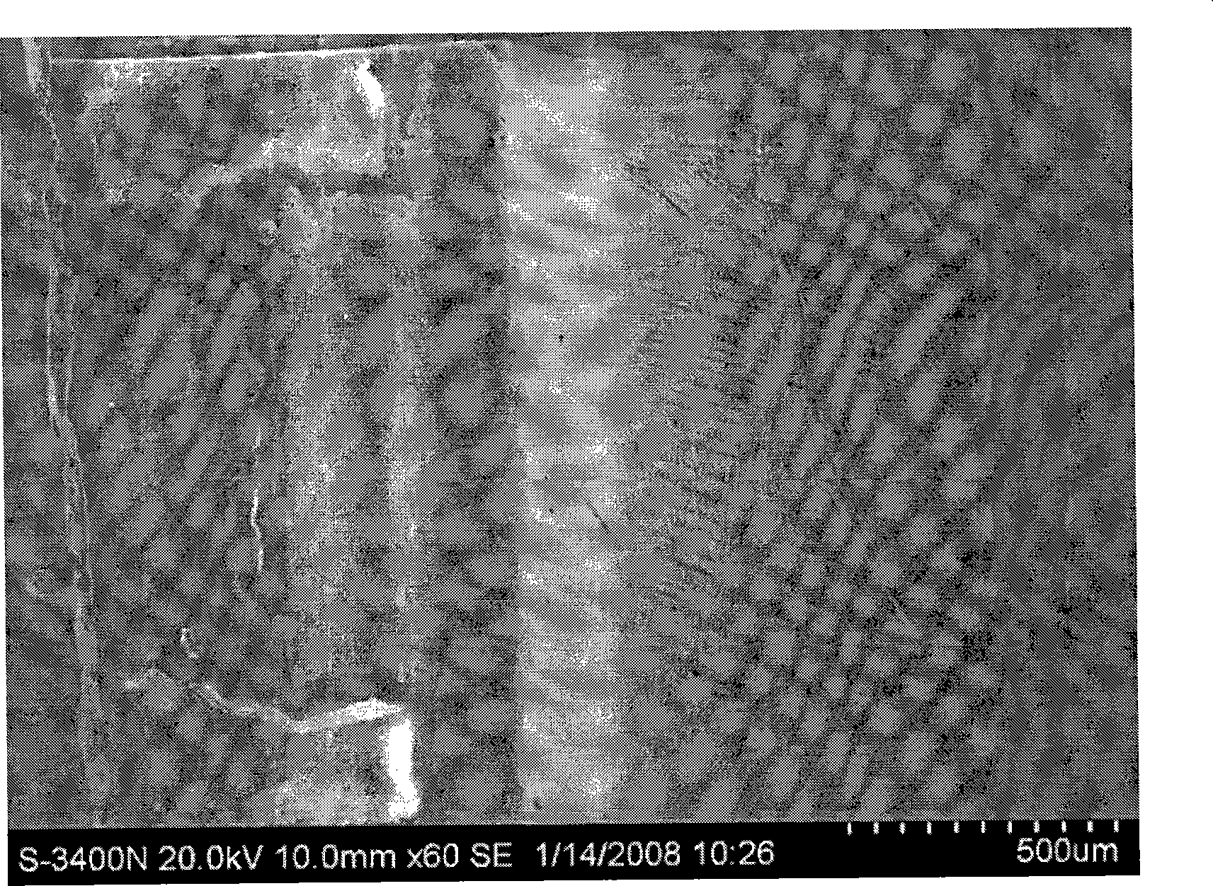
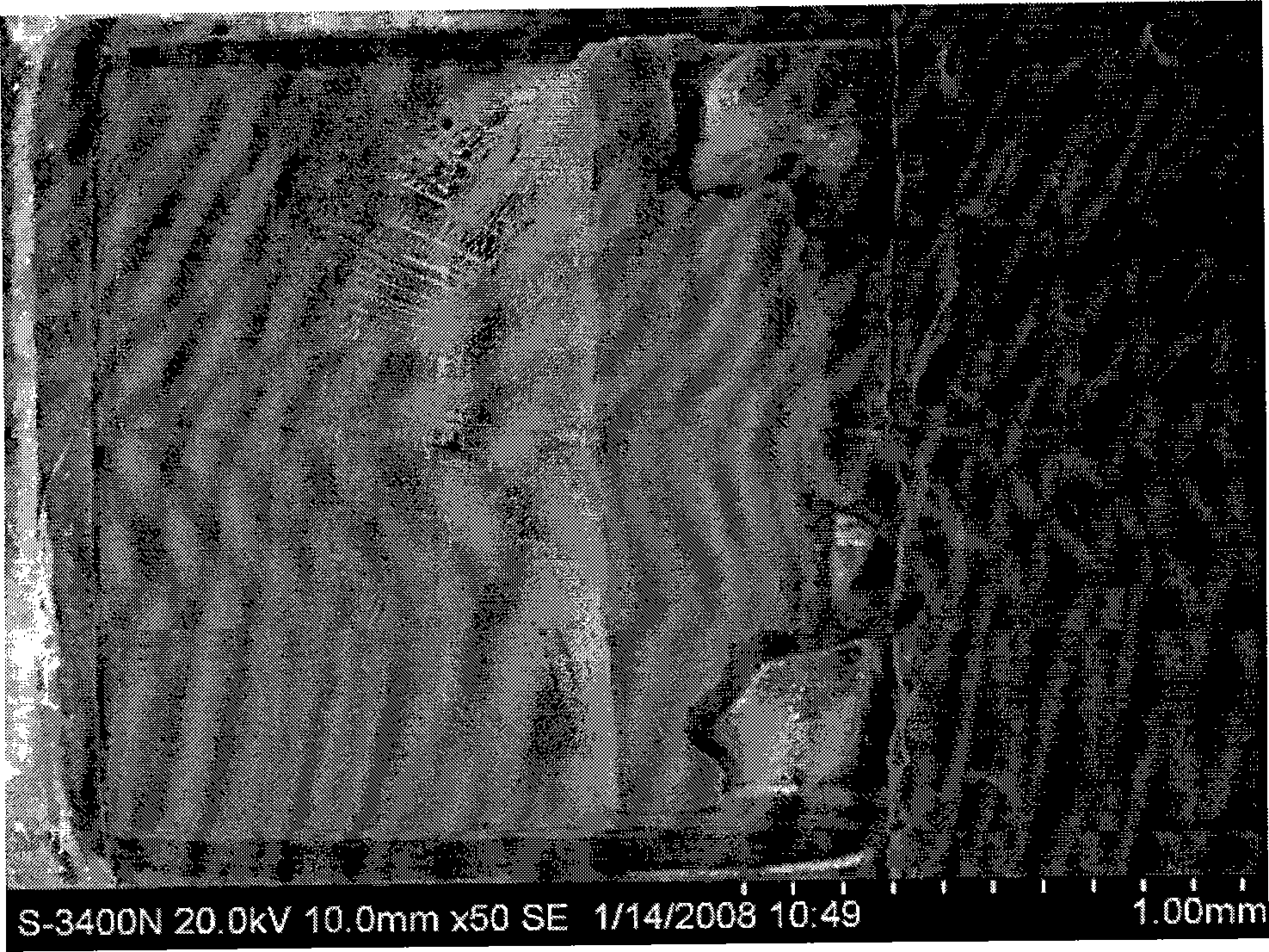
[0034] Embodiment 3: This embodiment uses lead-free solder Sn3.0Ag0.5CuP, and the flux is corrosive ZnCl 2 +NH 4 Cl+H 2 O solution, the brazing temperature is 260°C. The crystal crack test specimen is a cuboid with a volume of 20mm×12mm×3mm, the length of the middle groove is 16mm, the width is 4mm, and the depth is 2mm. After welding, it is naturally cooled in the air. After cooling, remove the residue on the surface of the solder joint to ensure the surface clean. Then magnify 10 times under a stereoscopic microscope to observe the crystallization cracks on the surface of the solder joints. The measured total length of the crack is half of the length of the brazing seam in the middle slot. Sn3.0Ag0.5CuP lead-free solder alloy has poor resistance to crystal cracking.

Embodiment 2

[0035] Embodiment 4: This embodiment uses lead-free solder Sn3.0Ag0.5CuCe, and the flux is corrosive ZnCl 2 +NH 4 Cl+H 2 O solution, the brazing temperature is 260°C. The crystal crack test specimen is a cuboid with a volume of 30mm×30mm×10mm, the length of the middle groove is 26mm, the width is 7mm, and the depth is 6mm. After welding, it is naturally cooled in the air. After cooling, remove the residue on the surface of the solder joint to ensure the surface clean. Then magnify 10 times under a stereoscopic microscope to observe the crystallization cracks on the surface of the solder joints. The measured total length of the crack is one-tenth of the length of the brazing seam in the middle slot. The ability of Sn3.0Ag0.5CuCe lead-free solder alloy to resist crystal cracking is average.

Embodiment 3

[0036] Embodiment 5: This embodiment uses lead-free solder Sn3.0Ag0.5CuGe, and the flux is corrosive ZnCl 2 +NH 4 Cl+H 2 O solution, the brazing temperature is 260°C. The crystal crack test specimen is a cuboid with a volume of 30mm×30mm×20mm, the length of the middle groove is 20mm, the width is 7mm, and the depth is 3mm. After welding, it is naturally cooled in the air. After cooling, remove the residue on the surface of the solder joint to ensure the surface clean. Then magnify 10 times under a stereoscopic microscope to observe the crystallization cracks on the surface of the solder joints. The measured total length of the crack is half of the length of the brazing seam in the middle slot. Sn3.0Ag0.5CuGe lead-free solder alloy has poor resistance to crystallization cracks.


PUM

PropertyMeasurementUnit
lengthaaaaaaaaaa
diameteraaaaaaaaaa
diameteraaaaaaaaaa

Abstract

A method and a device for testing and estimating a crystal crack of lead-free brazing filler metal welding spot, which belongs to a electronic packaging and lead-free solder fabrication filed of a micro-electronics industry. Because the size of a welding spot is getting smaller in the micro-electronics industry, crystal crack in a surface is hard to see and easy to ignore, the static strength and the endurance strength of a welding spot joint are leaded to decreasing. The invention get help from a style microscope which can be observed the crystal crack and the amount and total length of thecrystal crack, then opinion rating for the crystal crack is used for estimating the tendency or the sensibility of the crystal crack generated by the lead-free solder. The invention can reappear thecrystal crack generated in a braze welding process of the lead-free solder, then a physical simulation for the crystal crack of the lead-free solder is achieved, simultaneously, a braze welding temperature cycle and influence of crystal crack generated by the a geometric constraint of a soldered joint are researched and estimated.

Description

technical field [0001] The invention relates to a lead-free solder alloy brazing process performance evaluation technology in the field of electronic assembly lead-free brazing. Background technique [0002] Crystalline crack is a kind of process defect of grain boundary cracking caused by the restraint of solidification and shrinkage of solder alloy during the crystallization process of solder alloy. Therefore, the formation of crystallization crack is related to the mechanical behavior, grain boundary state and solidification process of the alloy during solidification. The characteristics of the process itself are related. Its formation mechanism can be explained by various theories such as liquid film theory and strength theory. It is generally believed that when the liquid alloy is cooled to the vicinity of the solidus line, a liquid film is formed around the grains. If the alloy solidifies and shrinks to generate a large enough stress and strain, the liquid film can b...

Claims


Application Information

Patent Timeline
Patent Type & Authority Patents(China)
IPC IPC(8): G01N21/88B23K3/00
Inventor 史耀武董文兴雷永平夏志东郭福李晓延刘建萍
Owner BEIJING UNIV OF TECH
Why Eureka
Try Eureka