Organic electroluminescent device

An electroluminescent element and organic technology, applied in electroluminescent light sources, electrical components, electric light sources, etc., can solve problems such as low stability, difficult operation, and reduced component performance, and achieve long life and less brightness reduction.

Inactive Publication Date: 2008-10-08
YAMAGATA PROMOTIONAL ORG FOR INDAL TECH
View PDF23 Cites 15 Cited by
  • Summary
  • Abstract
  • Description
  • Claims
  • Application Information

AI Technical Summary

Problems solved by technology

[0011] However, the electron-accepting dopants, Lewis acids, and electron-passing layer materials described in the above-mentioned Patent Documents 1 to 4 have low LUMO levels because electrons pass through the adjacent hole-transporting material HOMO (highest occupied molecular orbital). deep
Therefore, due to its high electron acceptability and sufficient reactivity, it is difficult to handle. Although a very small amount is mixed into other layers during evaporation or forms a trap level, the performance of the device is significantly reduced. In addition, due to its sufficient reactivity, it is difficult to synthesize The problem
[0012] In addition, even though the hole injection characteristics can be improved by the methods described in the above-mentioned Patent Documents 1 to 4, since the layer is formed of a material with high electron acceptability, there is still a problem in the stability of the device, and the driving life is not sufficient.
[0013] In this way, the driving life of the organic EL element is short, the stability is low, and it is a big problem as a light source such as a fax, a copier, a backlight of a liquid crystal display, and lighting. In addition, it is not preferable as a display element such as a full-color flat-panel display.

Method used


Image

  • Organic electroluminescent device
  • Organic electroluminescent device
  • Organic electroluminescent device

Examples


Embodiment 1

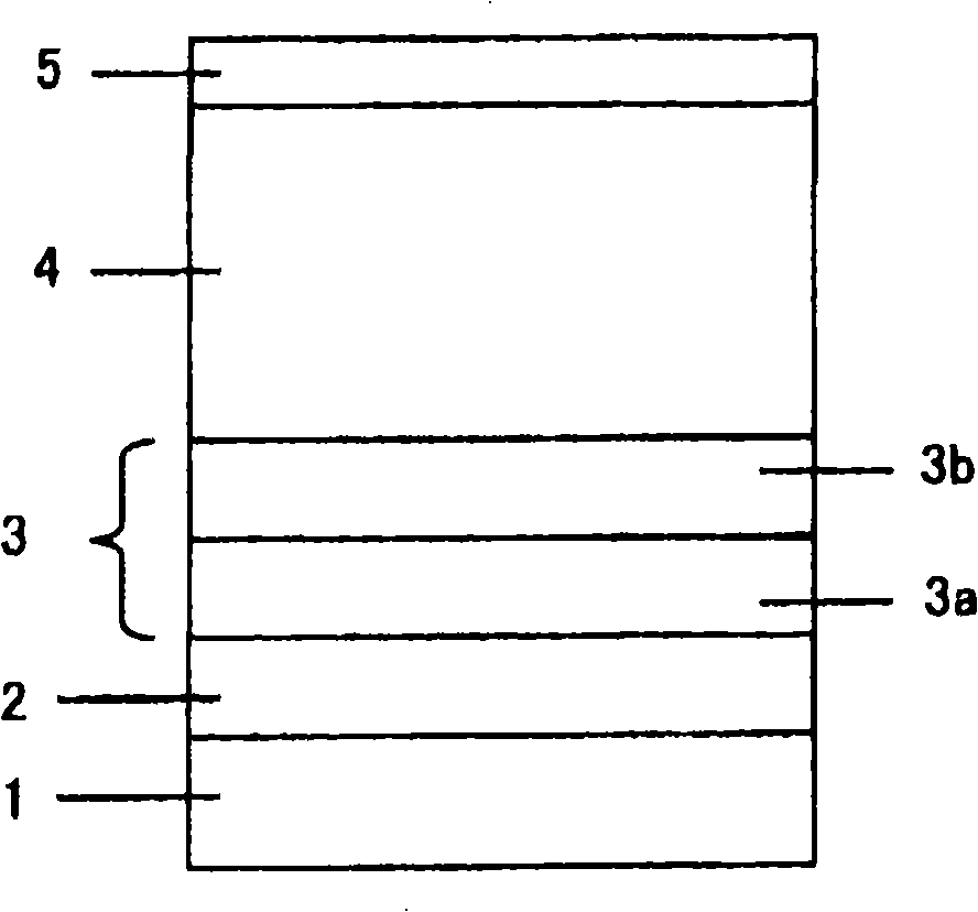
[0177] have Figure 5 An organic EL device with the basic structure shown was produced by the following method.

[0178] (formation of anode)

[0179] First, a 110 nm indium tin oxide (ITO) transparent conductive film is deposited on a glass substrate, and the deposited product (sputtered film product) is patterned with 2 mm wide stripes by normal photolithography and etching to form an anode.

[0180] For this patterned ITO substrate, ultrasonic cleaning by pure water and surfactant, running water washing by pure water, ultrasonic cleaning by a 1:1 mixed solution of pure water and isopropanol, washing by isopropanol The washing treatment was performed in the order of boiling washing with propanol. The substrate was slowly lifted from boiling isopropanol, dried in isopropanol vapor, and finally subjected to ultraviolet ozone washing.

[0181] The substrate was arranged in a vacuum evaporation device, and the inside of the device was exhausted to a vacuum degree of 5.0×10 us...

Embodiment 2

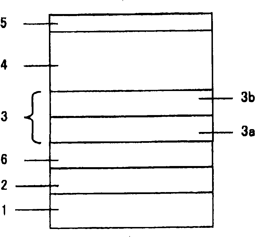
[0208] The molybdenum boat made of molybdenum that is added with the electron-transporting material (BAlq) shown in the following (chemical formula 18) is energized and heated, and the degree of vacuum is 1.9×10 -5 Pa, the evaporation rate is Evaporate on the anode ITO under the condition that the film thickness is 5nm, and change the film thickness from 10nm to 5nm on it. 3 An organic EL element was produced in the same manner as in Example 1 except that the domain of the first electron transporting material of Liq = 3:1.

[0209] [chemical formula 18]

[0210]

[0211] If the layer structure of the component is briefly expressed, it is:

[0212] ITO / BAlq(5nm) / Alq 3:Liq(5nm, 3:1) / Al(1.5nm) / α-NPD:MoO 3 (10nm, 4:1) / α-NPD(40nm) / Alq 3 : C545T (30nm, 100:1) / Alq 3 (34nm) / Alq 3 : Liq (10nm, 3:1) / Al (100nm).

Embodiment 3

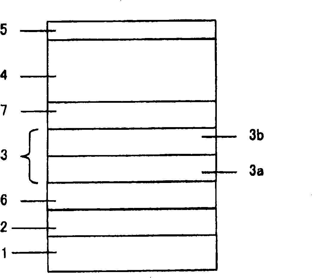
[0214] Between the region containing the first electron-transporting material and the region containing the first hole-transporting material, the degree of vacuum is 4.7×10 -5 Pa, the evaporation rate is Evaporated MoO with a film thickness of 10nm 3 , and an organic EL element was produced in the same manner as in Example 1 except that a hole transport layer containing α-NPD was formed in a film thickness of 30 nm.

[0215] If the layer structure of the component is briefly expressed, it is:

[0216] ITO / Alq 3 : Liq(10nm, 3:1) / Al(1.5nm) / MoO 3 (10nm) / α-NPD:MoO 3 (10nm, 4:1) / α-NPD(30nm) / Alq 3 : C545T (30nm, 100:1) / Alq 3 (34nm) / Alq 3 : Liq (10nm, 3:1) / Al (100nm).


PUM


Abstract

The present invention provides an organic electroluminescent device that can keep a stable luminescent characteristic for a long period. An organic electroluminescent device includes at least an anode 2, a charge generating layer 3, a luminescent layer 4 and a cathode 5 in this order. The charge generating layer 3 has an area 3a containing an electron transporting material at the anode side, and an area 3b containing a hole transporting material and a material capable of forming a charge transfer complex with the hole transporting material by an oxidation-reduction reaction at the cathode side, the hole transporting material and the material being laminated or mixed. The hole transporting material is in a radical cation state.

Description

technical field [0001] The present invention relates to life extension of organic electroluminescence elements (hereinafter referred to as organic EL elements). Background technique [0002] Organic EL elements are self-luminous elements that use organic compounds as light-emitting materials. Since they can emit light at a high speed, they are suitable for displaying moving images. They have the characteristics of simple element structure and can make the display panel thinner. Owing to having such excellent characteristics, organic EL elements are increasingly used in everyday life as displays for mobile phones and vehicles. [0003] However, this organic EL element has a problem that its driving life is shorter than that of an EL element containing an inorganic material. Specific phenomena that destabilize the driving of the element include a reduction in luminance of light emission, a voltage rise during constant current driving, and generation of non-light emitting port...

Claims


Application Information

Patent Timeline
Patent Type & Authority Applications(China)
IPC IPC(8): H01L51/50H01L51/54
CPCH01L51/5052H01L51/5084H01L51/0077H01L51/5278H01L51/0081H10K85/30H10K85/324H10K50/155H10K50/167H10K50/19H05B33/14C09K11/06H10K50/00
Inventor 中井敏光小田敦
Owner YAMAGATA PROMOTIONAL ORG FOR INDAL TECH
Why Eureka
Try Eureka