
Method of producing organic light emitting apparatus

An organic light-emitting device and a technology for organic light-emitting devices, which are used in electroluminescent light sources, semiconductor/solid-state device manufacturing, light sources, etc. Excellent drive durability characteristics, excellent placement durability characteristics, effect of non-uniformity elimination

Active Publication Date: 2011-05-11
CANON KK
View PDF3 Cites 0 Cited by
  • Summary
  • Abstract
  • Description
  • Claims
  • Application Information

AI Technical Summary

Problems solved by technology

However, under ambient pressure, the remaining contaminants and residues on the surface of the electrodes further increase, which even deteriorates the state compared to the state before cleaning
In addition, according to experiments conducted by the inventors, it was found that a pressure of 4.00 was too low to generate the required amount of ozone and active oxygen, and excellent driving durability characteristics could not be obtained

Method used


Image

  • Method of producing organic light emitting apparatus
  • Method of producing organic light emitting apparatus
  • Method of producing organic light emitting apparatus

Examples


example 1

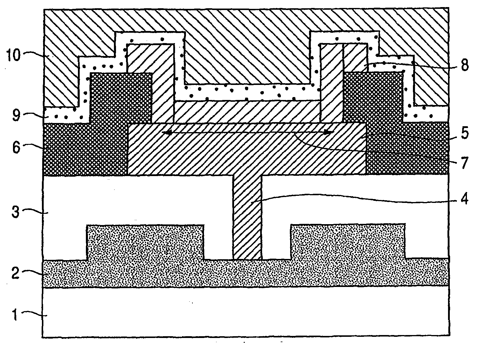
[0052] Using a positive photoresist polyimide resin, a device separation film with a thickness of 2 μm was formed over the entire surface of a substrate on which ITO formed on an Ag alloy film (thickness: 100 nm) was provided The film (thickness: 60 nm) was used as an anode (lower electrode). Then, the device separation film was patterned by exposing with a UV lamp followed by development, whereby opening portions were formed.

[0053] The device substrate thus obtained was cleaned with an aqueous solution of a surfactant, and rinsed with ion exchanged water and ultrasonic waves.

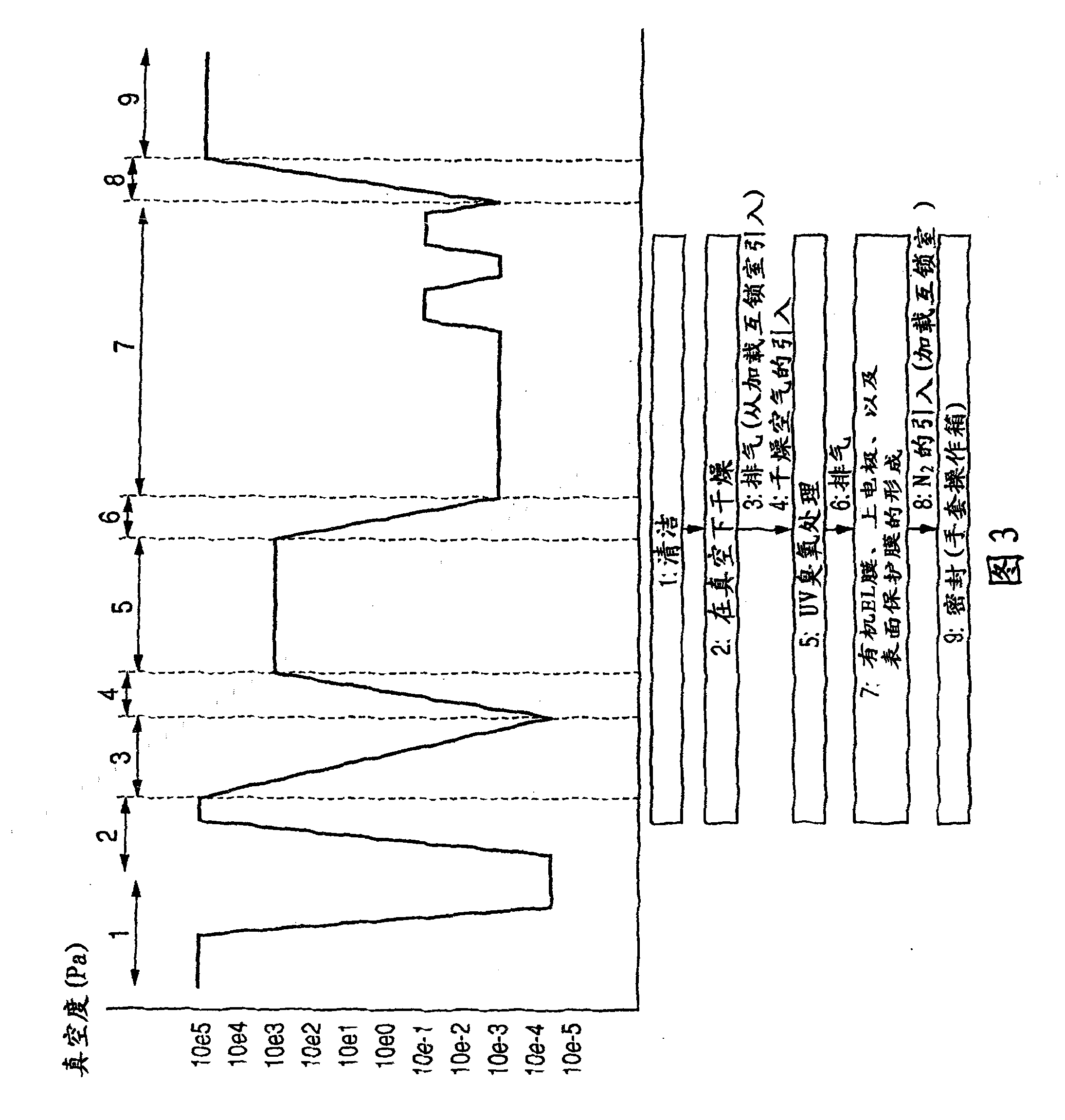
[0054] The cleaned device substrate was placed in a vacuum dryer to perform dehydration at 200° C. for 24 hours.

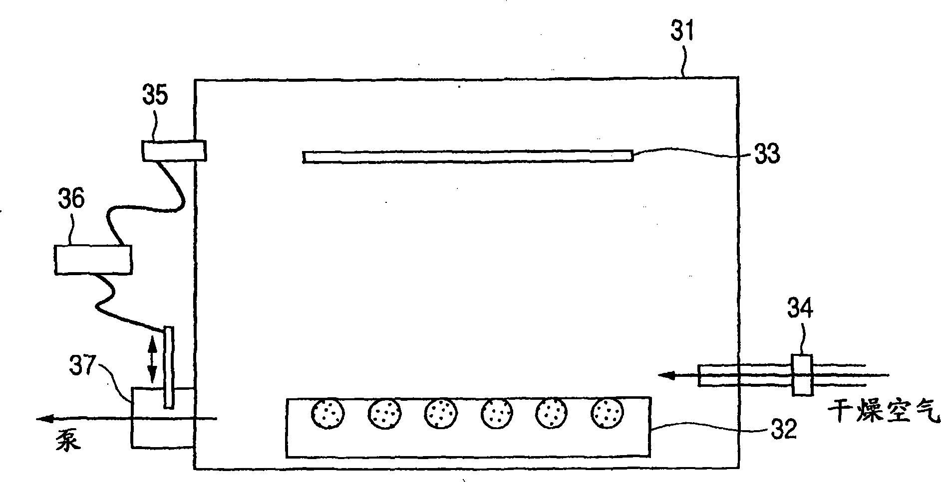
[0055] The device substrate subjected to dehydration was introduced into a substrate pretreatment apparatus, opposed to a low-pressure mercury lamp (output: 110 W), and was shaken at a rate of 20 mm / sec within a range of 50 mm intervals. The shortest distance between lamp and substrat...

example 2

[0064] A device substrate was fabricated in the same manner as in Example 1 except that a Cr film having a thickness of 100 nm was used as an anode, followed by cleaning and dehydration. Further, as a treatment before forming the organic EL layer, UV ozone treatment was performed in the same manner as in Example 1 except that the ambient pressure was set to 100 Pa.

[0065] The obtained organic light-emitting device was evaluated in the same manner as in Example 1, and it was found that L(100h) / L(ini) was 94.5% (initial illuminance L(ini)=1,050 cd / m 2 ), and the organic light-emitting device has excellent driving and lifetime characteristics, the same as Example 1. In addition, the luminescent state after being left at a temperature of 80° C. and a humidity of 80% for 1000 hours was the same as in the case before being left.

example 3

[0067] An organic light-emitting device was manufactured in the same manner as in Example 1, using the device substrate used in Example 1, except that the pressure during the process before forming the organic EL layer was 10000 Pa.

[0068] The obtained organic light-emitting device was evaluated in the same manner as in Example 1, and it was found that L(100h) / L(ini) was 92.8% (initial illuminance L(ini)=1,290cd / m 2 ), and the organic light-emitting device has excellent driving and lifetime characteristics, although slightly worse than those in Example 1. In addition, the luminescent state after being left at a temperature of 80° C. and a humidity of 80% for 1000 hours was the same as in the case before being left.


PUM


Abstract

A method for controlling a high-frequency radiator includes the steps of: (a) applying a high-frequency radiation through the solid-state oscillator and the antenna; (b) sensing part of the high-frequency radiation returned from the antenna to the solid-state oscillator; (c) adjusting radiation / propagation conditions for the high-frequency radiation on the basis of the sensed results in the step (b), the high-frequency radiation propagating from the solid-state oscillator to the antenna; and (d) after the step (c), applying the high-frequency radiation through the solid-state oscillator and the antenna to a target object.; In the step (c), the oscillation frequency of the solid-state oscillator, the power of the high-frequency radiation applied by the solid-state oscillator, the power supply voltage supplied to the solid-state oscillator, the impedance match between the output impedance of the solid-state oscillator and the impedance of the antenna, or any other condition is changed.

Description

technical field [0001] The present invention relates to a method of manufacturing an organic light emitting device that can be used for an image display device, a lighting system, and the like. Background technique [0002] In 1987, Tang et al. proposed an organic light-emitting device (organic EL (electroluminescence) device) having a configuration in which organic compounds having different carrier transport properties are stacked, and Holes and electrons are injected in good balance from the anode and cathode, respectively. Specifically, devices manufactured by setting the thickness of the organic compound layer (organic EL layer) to 200 nm or less have achieved 1000 cd / m at 10 V 2 The efficiency and illuminance have never been realized so far. [0003] Since then, attempts have been made so far to obtain high-illuminance luminescence at a lower voltage. For example, Japanese Patent Application Laid-Open No. H07-142168 discloses that an ITO anode is subjected to UV tre...

Claims


Application Information

Patent Timeline
Patent Type & Authority Patents(China)
IPC IPC(8): H01L51/56H05B33/10H05B33/22H05B33/14
Inventor 德永雄三大塚学真下精二远藤太郎西田直哉
Owner CANON KK
Learn More