GaN-based LED epitaxial wafer and preparation method thereof

A technology of LED epitaxial wafers and epitaxial wafers, which is applied in the direction of electrical components, circuits, semiconductor devices, etc., can solve the problems that it is difficult to obtain a p-type layer with high hole concentration, the performance of LEDs is difficult to further improve, and the forward voltage of GaN-based LEDs is high. High-performance preparation method, low cost, and precise preparation conditions

Inactive Publication Date: 2008-11-05
SOUTH CHINA NORMAL UNIVERSITY
View PDF1 Cites 15 Cited by
  • Summary
  • Abstract
  • Description
  • Claims
  • Application Information

AI Technical Summary

Problems solved by technology

Moreover, in order to reduce the resistance of the p-type layer, the thickness of the p-type layer of the LED epitaxial wafer should not exceed 0.5 μm, which makes it more difficul

Method used


Image

  • GaN-based LED epitaxial wafer and preparation method thereof
  • GaN-based LED epitaxial wafer and preparation method thereof
  • GaN-based LED epitaxial wafer and preparation method thereof

Examples


Embodiment 1

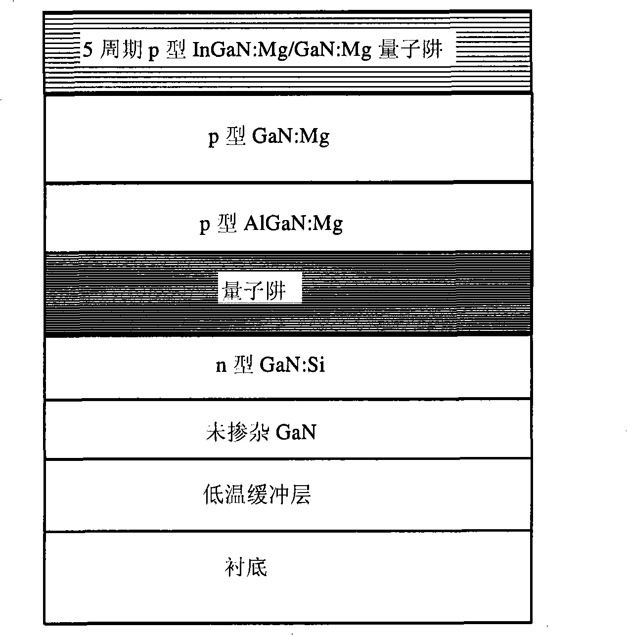
[0035] The structure of GaN-based LED epitaxial wafer with p-type contact layer is shown in the attached figure 1 As shown, from bottom to top are substrate, low temperature buffer layer, undoped GaN layer, n-type GaN layer, InGaN / GaN quantum well, p-type AlGaN and p-type GaN layer, p-type InGaN:Mg / GaN:Mg quantum well layer.

[0036] Its preparation method is:

[0037] (1) Using MOCVD equipment, heat up to 1000°C and bake the substrate for 10 minutes in a hydrogen atmosphere;

[0038] (2) Lower the temperature to 480°C, and grow a GaN low-temperature buffer layer with a thickness of 30nm on the substrate;

[0039] Raise the temperature to 1050°C to grow an undoped GaN layer with a thickness of 1.0μm;

[0040] (3) growing an n-type GaN:Si layer with a thickness of 2.0 μm at a temperature of 1000° C.;

[0041] (4) InGaN / GaN quantum wells were grown at 720°C, and the number of quantum well periods was 5;

[0042] (5) Raise the temperature to 1000°C to grow a p-type AlGaN:Mg...

Embodiment 2

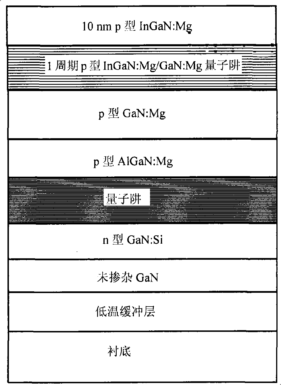
[0047] The structure of GaN-based LED epitaxial wafer with p-type contact layer is shown in the attached figure 2As shown, from bottom to top are substrate, low temperature buffer layer, undoped GaN layer, n-type GaN layer, InGaN / GaN quantum well, p-type AlGaN layer, p-type GaN, p-type InGaN:Mg / GaN:Mg Quantum well layer, p-type InGaN:Mg.

[0048] Its preparation method is:

[0049] (1) Using MOCVD equipment, heat up to 1000°C and bake the substrate for 10 minutes in a hydrogen atmosphere;

[0050] (2) Lower the temperature to 480°C, and grow a GaN low-temperature buffer layer with a thickness of 30nm on the substrate;

[0051] Raise the temperature to 1050°C to grow an undoped GaN layer with a thickness of 1.0μm;

[0052] (3) growing an n-type GaN:Si layer with a thickness of 2.0 μm at a temperature of 1000° C.;

[0053] (4) InGaN / GaN quantum wells were grown at 750°C, and the number of quantum well periods was 8;

[0054] (5) Raise the temperature to 1000°C to grow a p-...

Embodiment 3

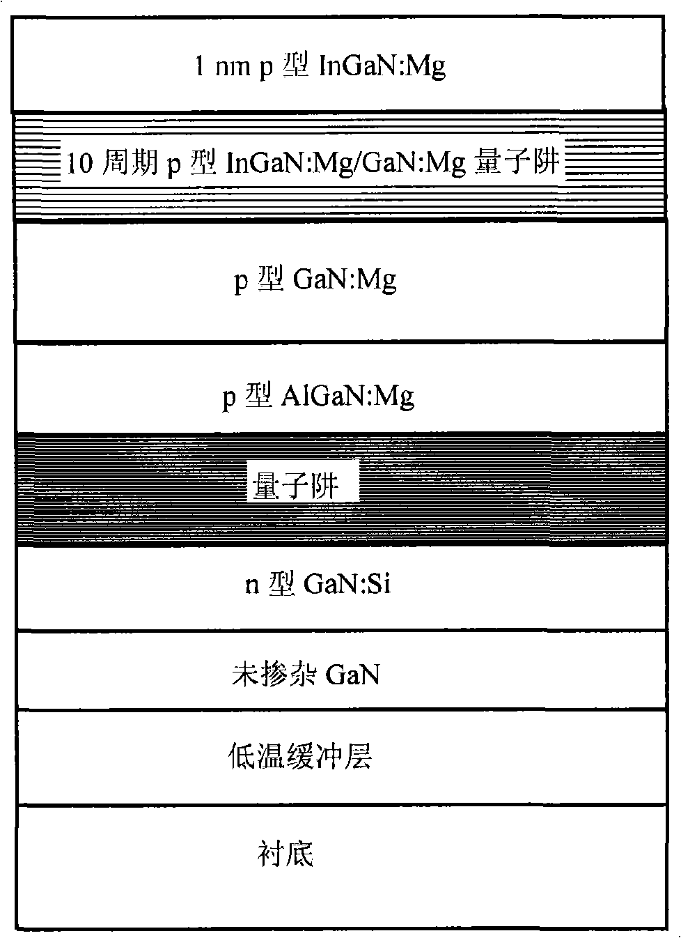
[0060] The structure of GaN-based LED epitaxial wafer with p-type contact layer is shown in the attached image 3 As shown, from bottom to top are substrate, low temperature buffer layer, undoped GaN layer, n-type GaN layer, InGaN / GaN quantum well, p-type AlGaN layer, p-type GaN, p-type InGaN:Mg / GaN:Mg Quantum well layer, p-type InGaN:Mg.

[0061] Its preparation method is:

[0062] (1) Using MOCVD equipment, heat up to 1000°C and bake the substrate for 10 minutes in a hydrogen atmosphere;

[0063] (2) Lower the temperature to 480°C, and grow a GaN low-temperature buffer layer with a thickness of 30nm on the substrate;

[0064] Raise the temperature to 1050°C to grow an undoped GaN layer with a thickness of 1.0μm;

[0065] (3) growing an n-type GaN:Si layer with a thickness of 2.0 μm at a temperature of 1000° C.;

[0066] (4) InGaN / GaN quantum wells were grown at 680°C, and the number of quantum well periods was 5;

[0067] (5) Raise the temperature to 1000°C to grow a p-...


PUM

PropertyMeasurementUnit
Thicknessaaaaaaaaaa
Thicknessaaaaaaaaaa
Thicknessaaaaaaaaaa

Abstract

The invention discloses a GaN base LED epitaxial wafer with the p-type contact layer and the preparation method, wherein the structure of the epitaxial wafer is a substrate, a low temperature buffer layer, an n-type layer, a quantum well, a p-type layer, a p-type contact layer in turn from the lower to the upper and the p-type contact layer is the quantum well layer structure. The invention is added with a p-type contact layer structure on the structure basis of the epitaxial wafer, wherein the p-type contact layer adopts the quantum well structure, due to the different energy of the well layer and the barrier layer valence band to effectively advance the hole density of the layer. Meanwhile, the motion of the hole on the direction vertical to the quantum well plane is restricted, which is favorable for the two-dimensional motion for the hole on the quantum well plane, under the applied voltage is favorable for the expansion in the p-type layer to cause the current distribution more uniform, to increase the performance of the LED. The preparation method of the epitaxial wafer provided in the invention is simple, low in cost, precise in the preparation condition, which realizes the industrialization production.

Description

technical field [0001] The invention belongs to the technical field of semiconductor optoelectronic devices, in particular to a GaN-based LED epitaxial wafer with a p-type contact layer and a preparation method thereof. Background technique [0002] GaN-based high-brightness light-emitting diodes (LEDs) are currently the frontier and hot spot in the global optoelectronics research and industry. The preparation of GaN-based LEDs needs to go through three main steps: LED epitaxial wafer growth, LED chip preparation and LED packaging. Among them, the preparation of LED epitaxial wafer is the core technology of LED, which plays a major role in the performance level of LED. [0003] The structure of the existing GaN-based LED epitaxial wafer is usually as attached Figure 5 As shown, it generally includes a substrate, a low-temperature buffer layer, an n-type layer, a quantum well, and a p-type layer. Wherein, the substrate material can be sapphire, SiC, Si, GaN and the like. ...

Claims


Application Information

Patent Timeline
IPC IPC(8): H01L33/00H01L33/06
Inventor 李述体
Owner SOUTH CHINA NORMAL UNIVERSITY
Why Eureka
Try Eureka