Manufacturing method of metal-coated polyimide substrate

A technology of polyimide substrate and manufacturing method, which is applied in the direction of semiconductor/solid-state device manufacturing, electrical components, circuits, etc., can solve the problems of increasing terminal pins and increasing the failure rate, and achieves the improvement of failure rate and industrial high value effect

Active Publication Date: 2009-01-21
SUMITOMO METAL MINING CO LTD
View PDF1 Cites 20 Cited by
  • Summary
  • Abstract
  • Description
  • Claims
  • Application Information

AI Technical Summary

Problems solved by technology

[0009] However, even in the case of using a metal-clad polyimide substrate with a metal layer formed by the above-mentioned sputtering method and plating method, for a COF with a

Method used


Image

  • Manufacturing method of metal-coated polyimide substrate

Examples


Embodiment 1

[0066] First, the polyimide sheet is made of Kapton 150EN (manufactured by Toray Dupont) using a magnetron sputtering device operating in a vacuum environment, and is carried out at 150°C in a chamber with a vacuum degree of 0.01 to 0.1Pa. minute heat treatment. Next, a nickel-chromium alloy layer with a thickness of 20 nm and a copper layer with a thickness of 300 nm were formed on the surface of the polyimide sheet using a nickel-chromium alloy target and a copper target containing 20% ​​by mass of chromium relative to the total amount. The surface resistance of the obtained metal coating was 0.1Ω / □.

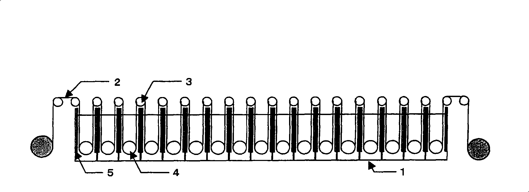
[0067] Then, using the obtained polyimide sheet after sputtering, using the above-mentioned continuous plating apparatus (number of plating tanks: 17 tanks), the copper plating layer was laminated on the copper film to obtain a metal-clad polyimide film with a copper conductor formed. Amine substrate. Here, as the anode of the above-mentioned continuous plating apparatus, a ...

Embodiment 2

[0070] Except that the ratio of the maximum value of the cathode current density in each electroplating tank to the minimum value is controlled to be 3, the same operation is performed as in Example 1, using the metal-clad polyimide substrate obtained, according to the above-mentioned "metal-clad polyimide "Evaluation method when the substrate is used as a COF", the occurrence rate of the positional deviation of the COF junction, the occurrence rate of the lead disconnection, and the occurrence rate of the tin plating film were calculated. The results are listed in Table 1.

Embodiment 3

[0072] The number of electroplating tanks of the above-mentioned continuous electroplating device is 12 tanks, and the total average current density is controlled to be 1.5A / dm 2 , and the ratio of the maximum value of the cathode current density in each electroplating tank to the minimum value is controlled to be 3, except that, the same operation as in Example 1, using the metal-clad polyimide substrate obtained, according to the above-mentioned "metal-clad "Evaluation method when polyimide substrate is used as COF" was used to obtain the defect rate of misalignment of the COF junction, the rate of lead disconnection, and the rate of tin plating peeling off. The results are listed in Table 1.


PUM

PropertyMeasurementUnit
Surface resistanceaaaaaaaaaa
Thicknessaaaaaaaaaa
Thicknessaaaaaaaaaa

Abstract

The invention provides a metal faced polyimide base plate manufacturing method capable of reducing the dimensional change dispersibility while heating the metal faced polyimide base plate, jointing stably under the endured heat quantity when used as COF and improving the qualification rate. The method comprises: a sputtering process for forming a metal coat on the polyimide sheet surface and an electroplating process for forming metallic conductor on the obtained metal coat by a continuous electroplating equipment. The invention is characterized in satisfying the (1) and (2) condition: (1) in the sputtering process, the surface resistivity of the formed metal coat is kept between 0.1/m2 and 1.0/m2; (2) in the electroplating process, the average cathode current density of all the electroplating bath is controlled between 1A/dm2 and 3A/dm2, and the ratio of the maximum of the cathode current density of all the electroplating bath to the minimum of that is controlled between 1 and 5, while the sheet conveying velocity is adjusted to 80-300m/h.

Description

technical field [0001] The present invention relates to a method of manufacturing a metal-clad polyimide substrate, and more specifically, to a method capable of reducing the dispersion of dimensional changes when a metal-clad polyimide substrate is heated, enabling stable bonding when used as a COF, And the manufacturing method of the metal-clad polyimide substrate that can improve the unqualified rate. Background technique [0002] In recent years, metal-clad polyimide substrates have been widely used as substrates for semiconductor packaging that encapsulate driving semiconductors that enable liquid crystal displays to display images. The polyimide sheet used in the above-mentioned metal-clad polyimide substrate has excellent heat resistance, and is not inferior to other plastic materials in terms of mechanical, electrical and chemical properties, so it is used as, for example, printed wiring boards. (PWB), flexible printed circuit board (FPC), tape for automatic tape bo...

Claims


Application Information

Patent Timeline
IPC IPC(8): H01L21/48H05K3/10
Inventor 大泷启一竹之内宏小笠原修一浅田雅男
Owner SUMITOMO METAL MINING CO LTD
Why Eureka
Try Eureka