Method for preparing nano CMOS integrated circuit by SiN masking technique

An integrated circuit and nanoscale technology, applied in the manufacture of circuits, electrical components, semiconductors/solid-state devices, etc., can solve the problems of waste of resources and energy, restrictions on the development of the semiconductor industry, and rising production costs, and achieve small conductive channels and realize The effect of leapfrog development and improvement of manufacturing capacity

Inactive Publication Date: 2009-02-04
XIDIAN UNIV
View PDF0 Cites 1 Cited by
  • Summary
  • Abstract
  • Description
  • Claims
  • Application Information

AI Technical Summary

Problems solved by technology

After years of accumulation, the world has invested more than one trillion US dollars in equipment and technology in the microelectronics industry. If the process technology is improved only through the replacement of equipment, a generation of equipment will be eliminated every 18 months, which will cause huge losses. The waste of resources and energy leads to an increase in production costs. Therefore, this situation seriously restricts the development of the semiconductor industry

Method used


Image

  • Method for preparing nano CMOS integrated circuit by SiN masking technique
  • Method for preparing nano CMOS integrated circuit by SiN masking technique
  • Method for preparing nano CMOS integrated circuit by SiN masking technique

Examples


Embodiment 1

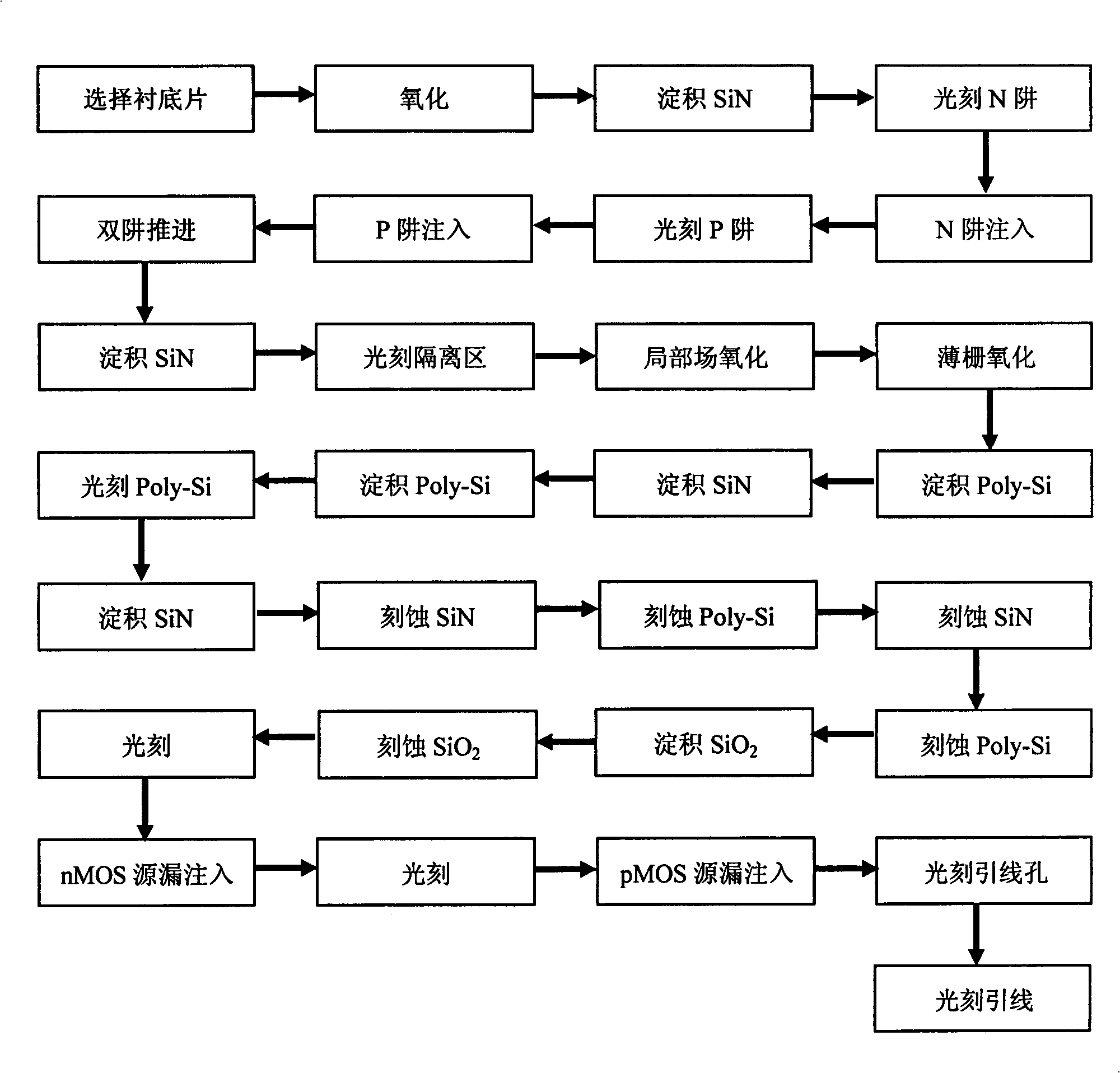
[0030] Embodiment 1: Prepare a CMOS integrated circuit with a 45nm conduction channel on a Si substrate. The specific steps are as follows:

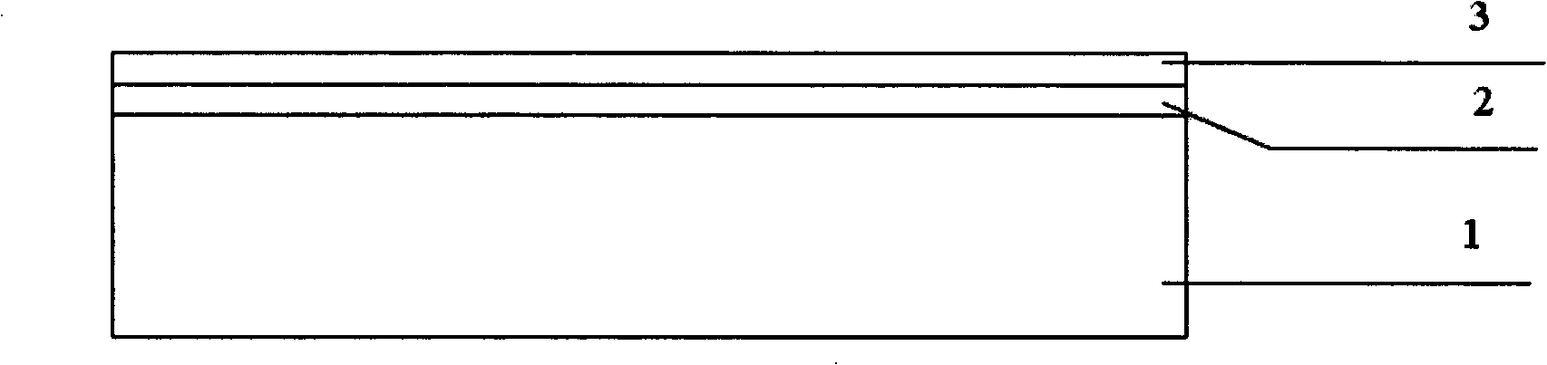
[0031] Step 1, deposit a masking layer, as shown in Figure 2(a).

[0032] (1a) Select the crystal orientation as and the doping concentration as 10 15 cm -3 Left and right p-type Si substrate sheet 1;

[0033] (1b) Thermally oxidize a layer of 40nm thick SiO on the substrate 2 Buffer layer 2;

[0034] (1c) In SiO 2 A 100nm thick SiN layer 3 is deposited on the buffer layer by a low pressure chemical vapor deposition LPCVD method, which is used for masking the implantation of the well region.

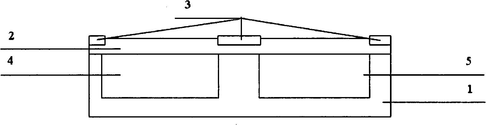
[0035] Step 2, forming a well region, as shown in Figure 2(b).

[0036] (2a) The P-well region 4 and the N-well region 5 are respectively lithographically etched on the SiN layer 3 in the order of phases;

[0037] (2b) Boron is implanted in the P-well region to form a p-type region, and the surface of the P-well region is thermally oxidized to form Si...

Embodiment 2

[0065] Embodiment 2: Prepare a CMOS integrated circuit with a 65nm conductive channel on an SOI substrate, the specific steps are as follows:

[0066] Step 1, deposit a masking layer, as shown in Figure 2(a).

[0067] (1a) Select the crystal orientation as and the doping concentration as 10 15 cm -3 Left and right p-type SOI substrate sheet 1;

[0068] (1b) Thermal oxidation of a layer of 40nm thick SiO on the substrate 2 Buffer layer 2;

[0069] (1c) In SiO 2 A 100nm thick SiN layer 3 is deposited on the buffer layer by APCVD method, which is used for the masking of the well region implantation.

[0070] Step 2, forming a well region, as shown in Figure 2(b).

[0071] (2a) Photoetching the P-well region 4 and the N-well region 5 on the SiN layer 3 in the order of phases;

[0072] (2b) Boron is implanted in the P-well region to form a p-type region, and the surface of the P-well region is thermally oxidized to form SiO 2 , P-well advancement is performed at the same time, and P-w...

Embodiment 3

[0100] Embodiment 3: Prepare a CMOS integrated circuit with a conduction channel of 90 nm on a Si substrate. The specific steps are as follows:

[0101] Step 1, deposit a masking layer, as shown in Figure 2(a).

[0102] (1a) Select the crystal orientation as and the doping concentration as 10 15 cm -3 Left and right p-type Si substrate sheet 1;

[0103](1b) Thermal oxidation of a layer of 40nm thick SiO on the substrate 2 Buffer layer 2;

[0104] (1c) In SiO 2 A 100nm thick SiN layer 3 is deposited on the buffer layer by means of plasma enhanced chemical vapor deposition (PECVD), which is used for masking the implantation of the well region.

[0105] Step 2, forming a well region, as shown in Figure 2(b).

[0106] (2a) Photoetching the P-well region 4 and the N-well region 5 on the SiN layer 3 in the order of phases;

[0107] (2b) Boron is implanted in the P-well region to form a p-type region, and the surface of the P-well region is thermally oxidized to form SiO 2 , P-well adva...


PUM


Abstract

The invention discloses a method based on SiN masking technique for fabricating a nano-scale CMOS integrated circuit. The process includes the following steps: fabricating an N/P well and growing a Poly-Si/SiN/Poly-Si multi-layer structure on the N/P well; etching the top layer of Poly-Si into a window and then depositing a layer of SiN; etching away the SiN on the surface of the substrate, except the SiN at the side wall of the Poly- Si; based on the etching ratio of Poly-Si to SiN(11:1), etching the Poly-Si on the surface of SiN; etching the SiN on surface of the substrate, except the SiN on the side wall of the SiN so as to expose the substrate of Poly-Si; based on the etching ratio of Poly-Si to SiN, etching the Poly-Si, except the Poly-Si in the protective area on the side wall of SiN so as to form an n/p MOSFET grid, and depositing a layer of SiO2 at the well area; injecting ions, self-aligning, and forming the source area and the drain area of the n/p MOSFET grid so as to form an n/p MOSFET device; and photoetching interconnection lines of the device so as to form a CMOS integrated circuit with a conducting channel at 45-90nm. The method can fabricate a CMOS integrated circuit which is improved in performance by 3-5 generations on a micron-scale Si integrated circuit processing platform without adding any funds and equipment investment.

Description

Technical field [0001] The invention belongs to the technical field of semiconductor integrated circuits, and in particular relates to a method for manufacturing nano-scale Si integrated circuits by using the existing micro-scale Si integrated circuit manufacturing process. Background technique [0002] The information industry is a pillar industry of the national economy. It serves various fields of the national economy. Microelectronics technology is the key to the information industry, and integrated circuits are even more critical. Since its inception in 1958, integrated circuits have developed at an alarming rate. They have become the core of information science and technology, the cornerstone of national economic development and national defense construction, and have had a huge impact on world politics, economy, and culture. As the fastest growing, most influential, and most widely used technology in human history, integrated circuits have become an important indicator of ...

Claims


Application Information

Patent Timeline
Patent Type & Authority Applications(China)
IPC IPC(8): H01L21/8238
Inventor 胡辉勇张鹤鸣戴显英宋建军舒斌宣荣喜赵丽霞王晓燕秦珊珊
Owner XIDIAN UNIV
Why Eureka
Try Eureka