MIM capacitor and manufacturing method thereof, semiconductor device and manufacturing method thereof

A manufacturing method and semiconductor technology, which are applied in the fields of semiconductor/solid-state device manufacturing, semiconductor devices, and semiconductor/solid-state device components, etc., can solve the problems of reduced capacitance performance, deterioration of capacitor capacitance performance, roughness of the lower plate 135b, etc. Improved performance, improved flatness effect

Inactive Publication Date: 2009-02-11
SEMICON MFG INT (SHANGHAI) CORP +1
View PDF2 Cites 12 Cited by
  • Summary
  • Abstract
  • Description
  • Claims
  • Application Information

AI Technical Summary

Problems solved by technology

[0009] In the method for manufacturing a semiconductor device with a MIM capacitor, the first metal layer 135 used to form the lower plate 135b of the MIM capacitor is generally made of aluminum, and the grain size of aluminum is relatively large, ranging from 0.5um to 4um. The formed lower pole plate 135b is relatively rough, and the flatness is poor, and then the flatness of the dielectric film 140b formed on

Method used


Image

  • MIM capacitor and manufacturing method thereof, semiconductor device and manufacturing method thereof
  • MIM capacitor and manufacturing method thereof, semiconductor device and manufacturing method thereof
  • MIM capacitor and manufacturing method thereof, semiconductor device and manufacturing method thereof

Examples


Example Embodiment

[0064] The specific embodiments of the present invention will be described in detail below with reference to the accompanying drawings.

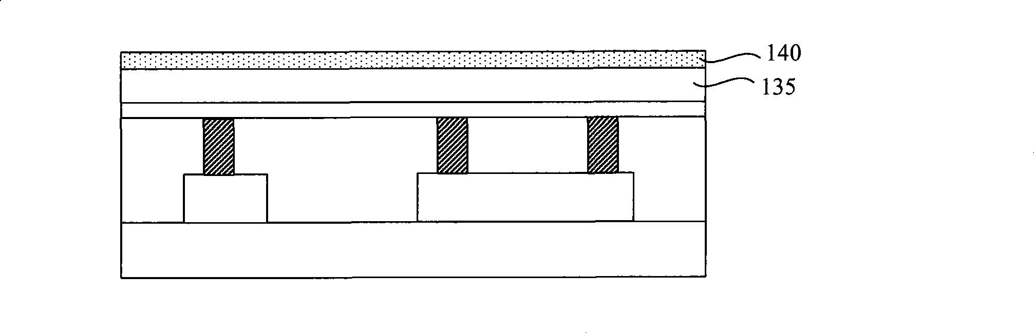
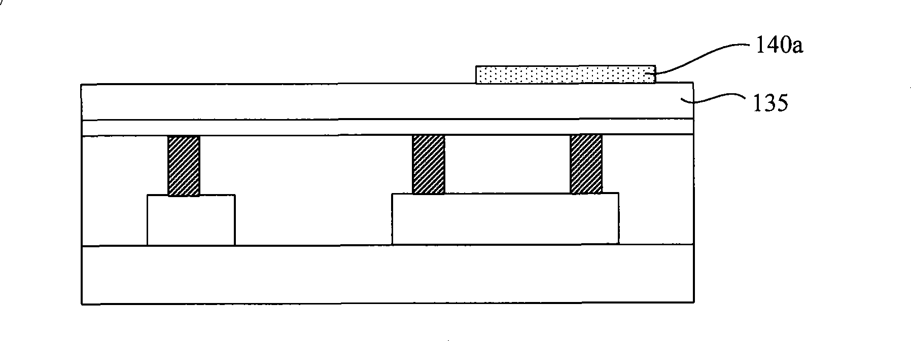
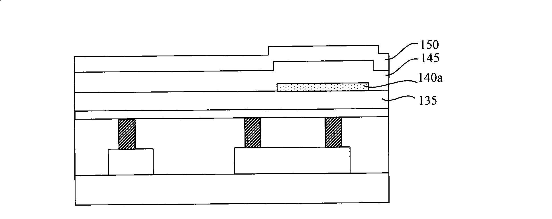
[0065] Figure 6 to Figure 10 It is a schematic cross-sectional view of the corresponding structure of each step of the embodiment of the manufacturing method of the MIM capacitor of the present invention.

[0066] Such as Figure 6 As shown, a semiconductor substrate 10 is provided, and an interconnection layer 12 is formed in the semiconductor substrate 10; the surface of the interconnection layer 12 is exposed, and the material of the interconnection layer 12 may be copper or aluminum; except for the interconnection Outside the surface area of ​​the layer 12, the surface of the semiconductor substrate 10 is made of insulating material, and the insulating material can be silicon oxide, silicon nitride, silicon carbide, silicon oxycarbon compound, silicon carbon nitride, fluorosilicone glass, phosphorous silicon One of glass, borosilicate glass...


PUM


Abstract

A manufacturing method of an MIM capacitor comprises the following steps: providing a semiconductor substrate; forming a first metal layer on the semiconductor substrate; forming a second metal layer on the first metal layer, and leveling the second metal layer; forming a dielectric layer on the second metal layer; forming a third metal layer on the dielectric layer; and patterning the third metal layer, the dielectric layer, the second metal layer and the first metal layer to form the MIM capacitor with a first metal layer pattern and a second metal layer pattern as a lower polar plate, a third metal layer pattern as an upper polar plate and a dielectric layer pattern as a dielectric medium. The invention also provides an MIM capacitor, as well as a semiconductor device and a manufacturing method thereof. The invention can improve the flatness of the lower polar plate of the MIM capacitor.

Description

technical field [0001] The invention relates to the technical field of semiconductor manufacturing, in particular to a metal-insulator-metal (Metal-Insulator-Metal, MIM) capacitor and a manufacturing method thereof, a semiconductor device including the MIM capacitor and a manufacturing method thereof. Background technique [0002] MIM capacitors have the advantages of high capacity and low resistivity, and are widely used in radio frequency circuits or high-speed analog circuits. MIM capacitors also have good matching characteristics with copper interconnect structures and are often fabricated integrally with copper interconnect structures. The Chinese patent application document with the patent publication number CN 1627477A (published on June 15, 2005) discloses a method for manufacturing a semiconductor device with a MIM capacitor. [0003] Figure 1 to Figure 4 It is a schematic cross-sectional view of each step of the manufacturing method of a semiconductor device with...

Claims


Application Information

Patent Timeline
IPC IPC(8): H01L21/02H01L21/28H01L21/822H01L21/768H01L29/92H01L27/04H01L23/522
Inventor 胡友存
Owner SEMICON MFG INT (SHANGHAI) CORP
Why Eureka
Try Eureka