Nickel or nickel base alloy electrode sheet type resistor and method of producing the same

A technology of nickel-based alloy and manufacturing method, applied in resistance manufacturing, non-adjustable metal resistors, resistors, etc., can solve problems such as chip resistor failures

Inactive Publication Date: 2009-02-18
杨金波 +1
View PDF0 Cites 12 Cited by
  • Summary
  • Abstract
  • Description
  • Claims
  • Application Information

AI Technical Summary

Problems solved by technology

[0007] In actual use, the chip resistors made by this method can easily cause the electroplated nickel layers 7a, 7b to separate from the upper electrode layers 3a, 3b due to the high temperature during soldering, and cause the tin solder of the resistor to be separated from the upper electrode layers. 3a, 3b chemical reaction occurs, leading to chip resistor failure

Method used


Image

  • Nickel or nickel base alloy electrode sheet type resistor and method of producing the same
  • Nickel or nickel base alloy electrode sheet type resistor and method of producing the same
  • Nickel or nickel base alloy electrode sheet type resistor and method of producing the same

Examples


Embodiment 1

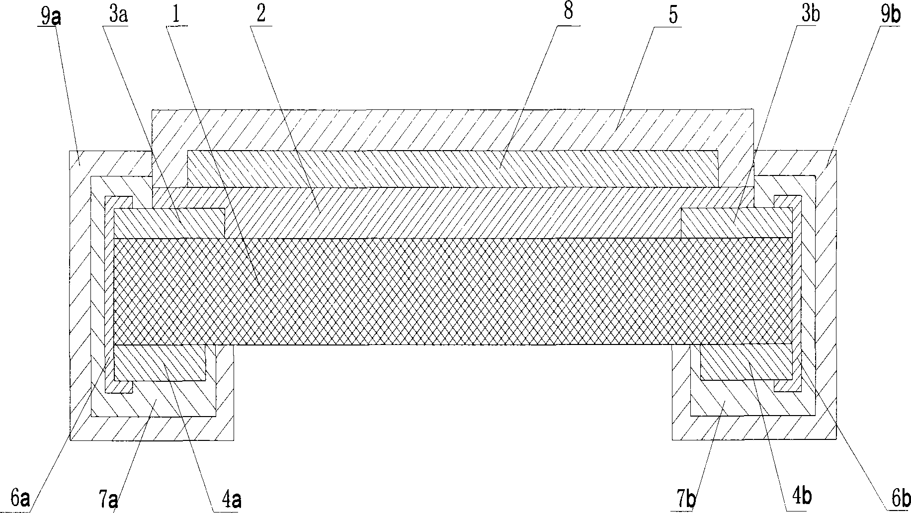
[0031] figure 2 It is a cross-sectional view of a nickel or nickel-based alloy electrode thick-film chip resistor according to Example 1 of the present invention. In this figure, 1 is the insulating substrate of the present invention, 2 is the resistance layer of the present invention, 3a, 3b are the electrode layers at both ends of the front side of the present invention, and the resistance layer 2 is made of ruthenium oxide paste by screen printing Materials are printed on the insulating substrate 1 and sintered. After that, the mask patterns of the electrode layers 3a and 3b at both ends of the front and the electrode layers 4a and 4b at both ends of the back are formed by screen printing. The alloy method is to form the electrode layers 3a, 3b at both ends on the upper side, and the electrode layers 4a, 4b at both ends on the back, and then form the electrode layers 6a, 6b at both ends of the side by vacuum arc ion plating, and then use the electroplating process to form ...

Embodiment 2

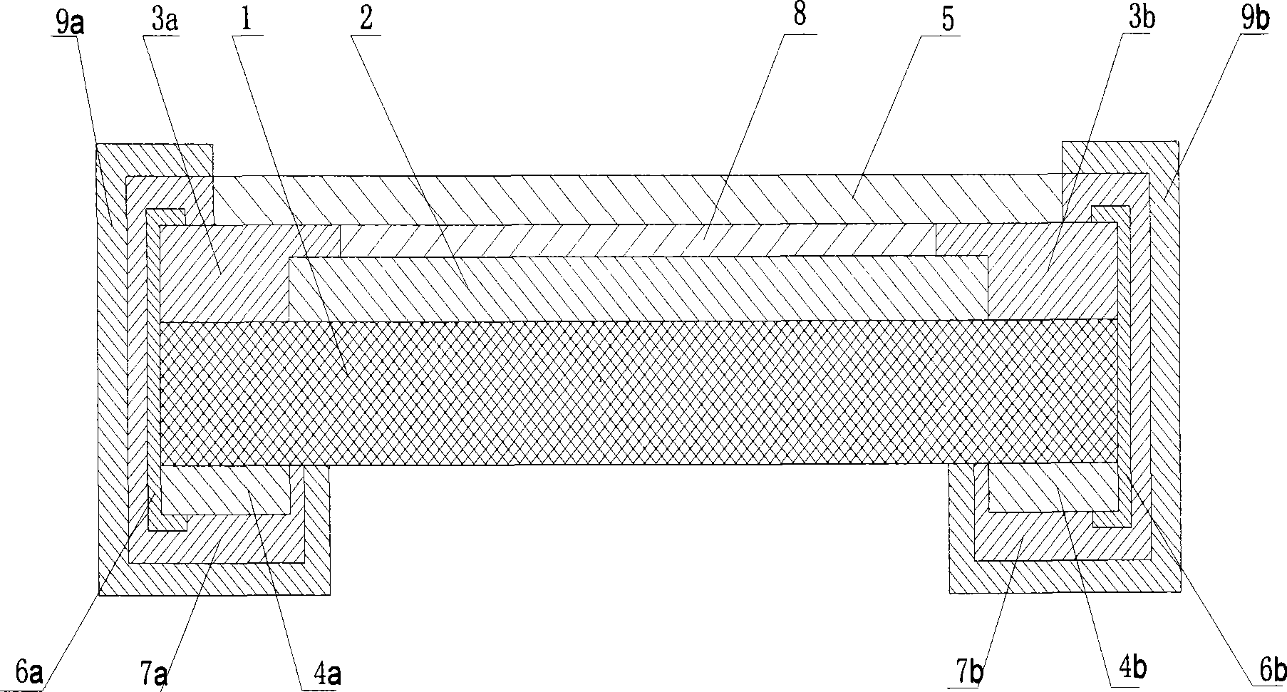
[0045] Figure 4 It is a sectional view of nickel or nickel-based alloy thick film chip resistor of embodiment 2 of the present invention, Figure 5 It is the manufacturing flow chart of the nickel or nickel-based alloy thick film chip resistor of the embodiment 2 of the present invention.

[0046] Since the manufacture of the chip resistor directly adopts nickel or nickel-based alloy as the electrode material, the nickel plating process in Example 1 can be omitted, and the electrode layer 3a, 3b on the upper surface and the end electrode layer 6a can be formed directly by electroplating. , 6b, the surface of the back electrode layer 4a, 4b is directly tin-plated as a solder layer.

Embodiment 3

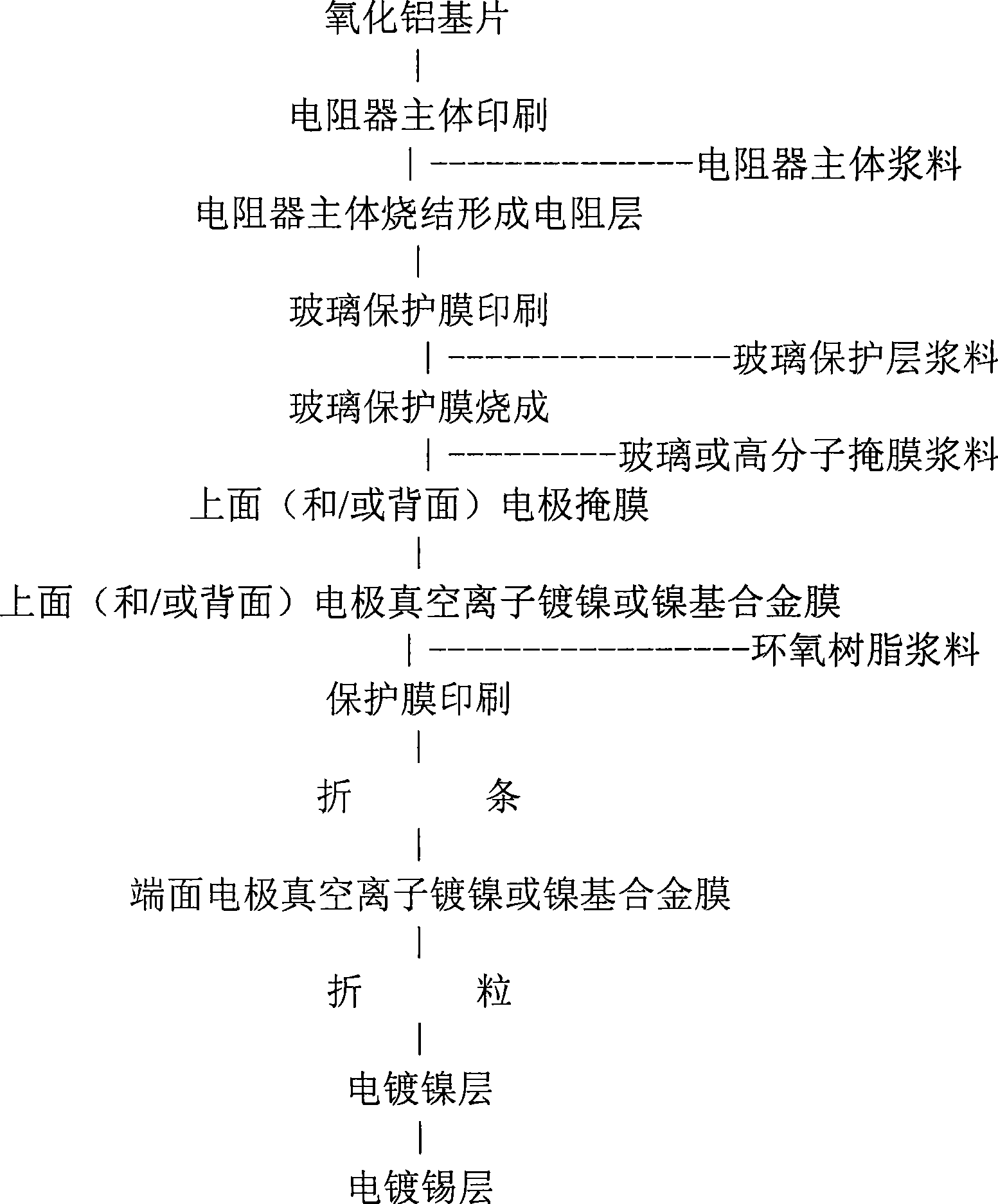
[0048] Image 6 It is the sectional view of the nickel or nickel-base alloy thin film chip resistor of embodiment 3, Figure 7 It is the manufacturing flowchart of the nickel or nickel-base alloy thin film chip resistor of embodiment 3

[0049] Combine below Image 6 Figure 7 The manufacturing method of the nickel or nickel-based alloy thin film chip resistor of embodiment 3 is described in detail. The resistance layer 2 of this example no longer uses the film-forming method of screen printing thick film technology, but uses NiCr and / or NiCrSi as the resistance material of the resistance layer to form the resistance layer 2 by vacuum sputtering. First, use a screen printing mask to make a resistance pattern, and then sputter to form a resistance layer; then use screen printing to form a mask pattern of the electrode layers 3a, 3b at both ends on the top, and the electrode layers 4a, 4b at both ends on the back, using vacuum arc The method of ion plating nickel or nickel-b...


PUM


Abstract

The invention discloses an electrode chip resistor of nickel or nickel base alloy and manufacture method thereof, which is invented for solving the problem that a chip resistor fault is easy to produce in the prior art. The resistor comprises an insulating substrate, on at least one side of which is formed with a resistor layer, and a pair of upper electrode layers formed at least on the upper of the resistor layer terminal and the upper of the insulating substrate, the resistor layer and the electrode layers are jointed together by physical joint between metal and metal, the electrode layers are nickel or nickel base alloy layers. The resistor formed adopting this method does not generate phenomenons of metallic layer separation and chemical reaction in actual use, because of using nickel or nickel base alloy to replace silver as electrode, not only can completely satisfy requirement of electric performance of the resistor, but also can reduce the processing procedure, greatly improves reliability of resistor use, the chip resistor of good electric performance can be manufactured with high efficiency and low cost.

Description

technical field [0001] The invention relates to a chip resistor and a manufacturing method thereof. Background technique [0002] With the development of small electronic devices such as mobile phones, notebook computers, MP3, and MP4 in recent years, the demand for small electronic components widely used in electronic circuits is also increasing. Chip resistors are one of the small electronic components, which are widely used in various small electronic devices. [0003] The traditional manufacturing of chip resistors is to form the electrode layers at both ends on the insulating substrate by screen printing, and then sinter at a temperature of 800°C-1000°C to form the silver electrodes at both ends of the insulating substrate. Thereafter, a resistance layer is formed by screen-printing ruthenium oxide paste on the blank areas of the electrode layers at both ends of the upper surface, and then sintered at a temperature of 800°C-1000°C to form a resistance layer. In order ...

Claims


Application Information

Patent Timeline
Patent Type & Authority Applications(China)
IPC IPC(8): H01C7/00H01C1/14H01C17/00H01C17/12H01C17/28
CPCH01C17/006H01C17/06
Inventor 杨金波王鑫培
Owner 杨金波
Why Eureka
Try Eureka