
Method for detecting whether present layer aligning with anterior layer of chip

A technology for detecting chips and current layers, applied in the direction of semiconductor/solid-state device testing/measurement, etc., can solve the problems of chip waste manpower and material resources, chip deformation, chip performance degradation, etc., to save manpower and material resources, improve production efficiency, improve performance effect

Inactive Publication Date: 2009-02-18
SEMICON MFG INT (SHANGHAI) CORP
View PDF0 Cites 1 Cited by
  • Summary
  • Abstract
  • Description
  • Claims
  • Application Information

AI Technical Summary

Problems solved by technology

[0006] Leakage of water and oxygen will cause chip deformation, affect the performance of the chip, and may cause chip scrapping; the reduction of chip performance will reduce the production efficiency of the factory; chip scrapping wastes manpower and material resources

Method used


Image

  • Method for detecting whether present layer aligning with anterior layer of chip
  • Method for detecting whether present layer aligning with anterior layer of chip
  • Method for detecting whether present layer aligning with anterior layer of chip

Examples


Embodiment Construction

[0016] The present invention will be described in further detail below in conjunction with the accompanying drawings.

[0017] An embodiment of the present invention is aimed at solving the problem of water and oxygen leakage from the machine caused by chip deformation when growing silicon nitride in the machine.

[0018] Figure 4 It is a flow chart of steps of the present invention. Such as Figure 4 As shown, the present invention comprises the following steps: Step 1, mark on the surface of the wafer to be tested, and expose the wafer to be tested in the lithography area to expose the marks of the current layer and the contrast layer; Step 2, use an overlay measuring instrument to measure the current layer And the marking of the control layer, and use the analysis software of the overlay measuring instrument to perform simulation calculations, and judge whether there is deformation through the measurement results.

[0019] The present invention needs to use an overlay m...


PUM


Abstract

A method for detecting whether a current layer of a chip is aligned with a front layer of the chip or not, belonging to a semiconductor process manufacturing field, comprises marking a wafer surface to be detected, exposing markers of the current layer and the contrast layer of a micro-shadow zone of the wafer to be detected; measuring the markers of the current layer and the contrast layer by an overlapping measuring apparatus and performing analog computation by an analysis software of the overlapping measuring apparatus, judging whether deformation is existed by a measured result. The invention solves the problem that the chip is deformed, improves performance of the chip and production efficiency of the factory, saves manpower and material resources.

Description

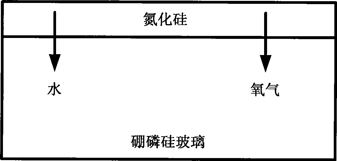
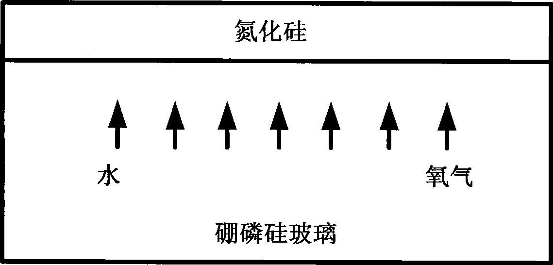
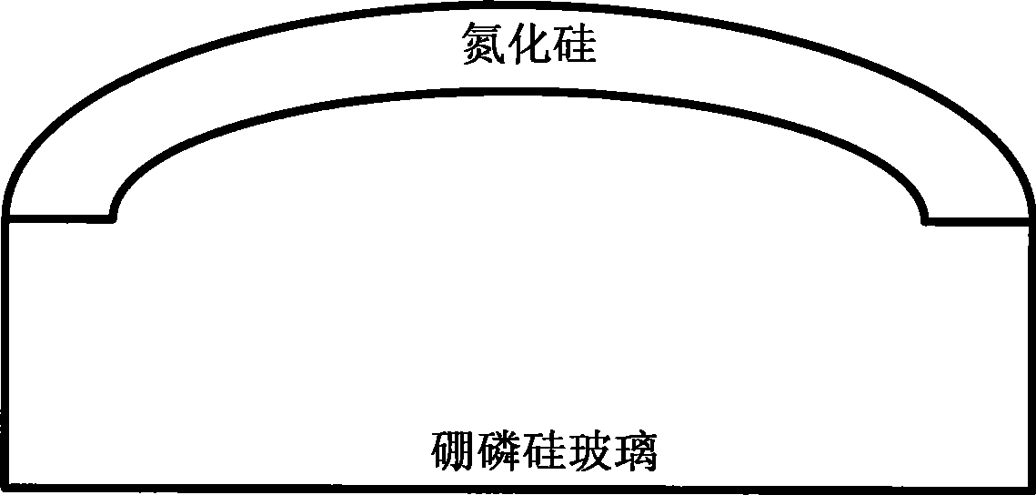
technical field [0001] The invention relates to the field of semiconductor technology, in particular to a method for detecting whether the current layer of a chip is aligned with the previous layer. Background technique [0002] Distortion refers to a certain kind of crystal crack damage displacement. In the semiconductor process, it often happens that the current layer of the chip is deformed and cannot be aligned with the previous layer. For example, during the process of growing silicon nitride, there are associated deformations in the chip. [0003] figure 1 is a schematic diagram of water and oxygen leakage. Such as figure 1 As shown, when the chip grows silicon nitride in the machine, a little water and oxygen leak out of the machine, and the leaked water and oxygen invade into the bottom borophosphosilicate glass of the chip. [0004] figure 2 It is a schematic diagram of water and oxygen volatilization. Such as figure 2 As shown, in the subsequent high-temp...

Claims


Application Information

Patent Timeline
IPC IPC(8): H01L21/66
Inventor 梁国亮杨金坡郭伟凯高莲花
Owner SEMICON MFG INT (SHANGHAI) CORP
Learn More