

Process for growing ZnO thin-film on Si substrate
A substrate and thin film technology, which is applied in electrical components, semiconductor/solid-state device manufacturing, circuits, etc., can solve problems such as lattice mismatch, Si substrate surface oxidation, and large thermal mismatch, so as to solve the problem of heat dissipation and improve Good performance and heat dissipation
- Summary
- Abstract
- Description
- Claims
- Application Information
AI Technical Summary
Problems solved by technology
Method used
Image

Examples
preparation example Construction
[0030] The present invention will be described in detail below in conjunction with the preparation method of the present invention and the accompanying drawings.
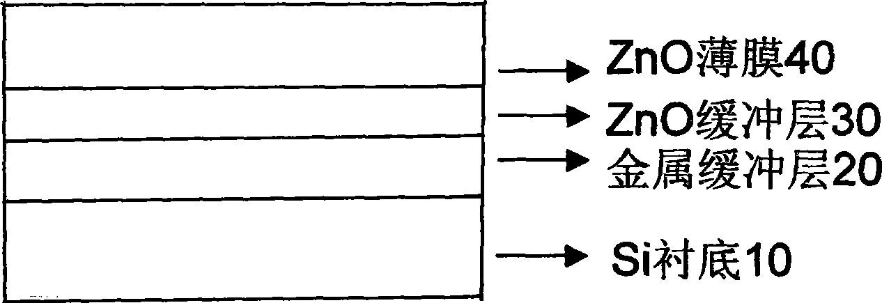
[0031] see figure 1 Shown, a kind of method of growing ZnO film on Si substrate of the present invention is characterized in that, comprises the following steps:
[0032] Step 1: use chemical cleaning method to clean the surface of Si substrate 10, and use hydrofluoric acid etching method to remove the oxide layer on its surface, described Si substrate 10 includes: (001), (011) or (111 ) crystal-oriented Si substrate;
[0033] Step 2: Put the cleaned Si substrate 10 into the deposition equipment, evaporate a layer of metal buffer layer 20, the metal buffer layer 20 includes: gold, silver, aluminum or magnesium, the thickness of the metal buffer layer 20 0.5-10 μm, and the deposition equipment for evaporating metal is physical vapor deposition equipment;
[0034] Step 3: Put the Si substrate 10 covering the metal ...
Embodiment 1
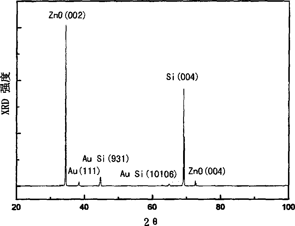
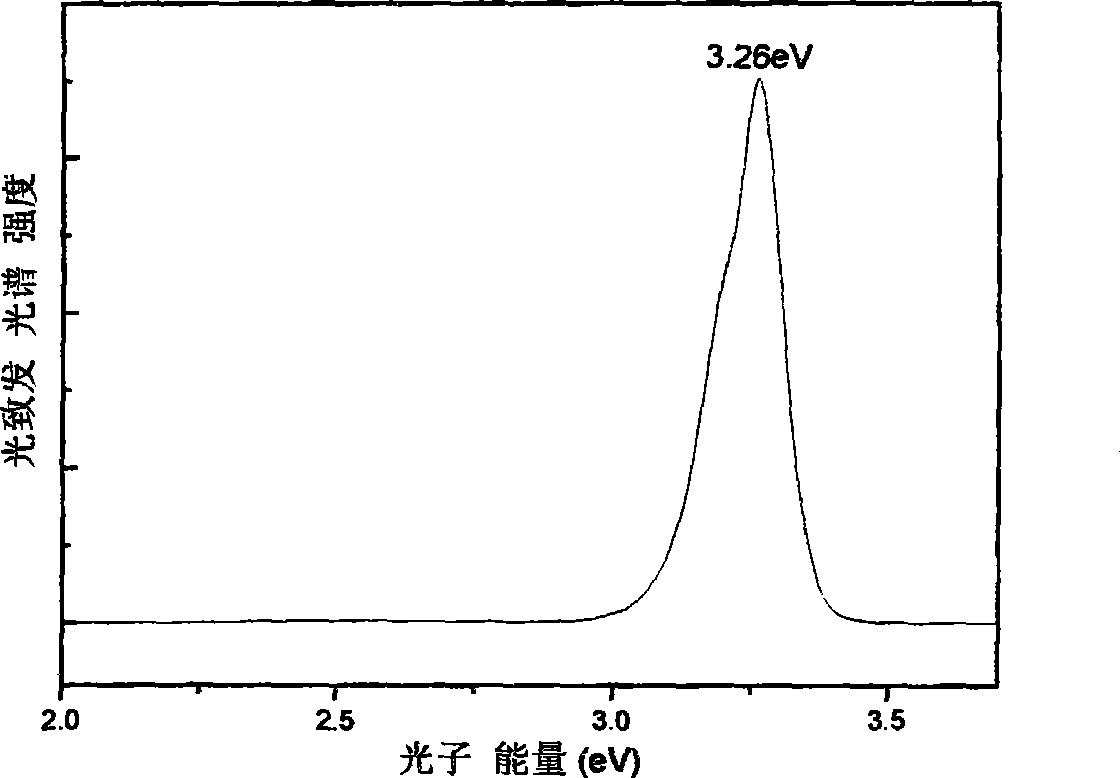
[0037] The specific steps of growing a ZnO thin film after evaporating metal Au on the Si substrate 10 of (001) crystal orientation are as follows (in conjunction with referring to figure 1 ):
[0038] Clean the surface of the Si substrate 10 with the (001) crystal orientation by a chemical cleaning method, and remove the oxide layer on the surface by hydrofluoric acid etching, so that the Si substrate 10 with the (001) crystal orientation is in a dehydrated state;
[0039] A layer of 850nm metal Au buffer layer was evaporated by physical vapor deposition method on the cleaned Si substrate 10 with (001) crystal orientation. During evaporation, the Si substrate 10 with (001) crystal orientation had a temperature of 150° C. and an air pressure of 4 ×10 -3 Pa;
[0040] Fix the Si substrate 10 with the (001) crystal orientation evaporated with the metal Au buffer layer on the substrate holder, and slowly put it into the growth equipment to grow the ZnO thin film. The growth equ...
Embodiment 2
[0045] The specific steps of growing a ZnO thin film after evaporating metal Au on the Si substrate 10 of (110) crystal orientation are as follows (in conjunction with referring to figure 1 ):
[0046] 1. Clean the surface of the Si substrate 10 with (110) crystal orientation by chemical cleaning method, and remove the oxide layer on the surface by hydrofluoric acid etching, so that the Si substrate 10 with (110) crystal orientation is in a dehydrated state ;
[0047] 2. Evaporate a layer of 750nm metal Au buffer layer by physical vapor deposition on the cleaned Si substrate 10 with (110) orientation. During evaporation, the temperature of Si substrate 10 with (110) orientation is 100° C. 4×10 -3 Pa;
[0048] 3. Fix the Si substrate 10 with the (110) crystal orientation evaporated with the metal Au buffer layer on the substrate holder, and slowly put it into the growth equipment to grow the ZnO thin film. The growth equipment used is a self-developed chemical vapor deposit...
PUM
| Property | Measurement | Unit |
|---|---|---|
| thickness | aaaaa | aaaaa |
| temperature | aaaaa | aaaaa |
| thickness | aaaaa | aaaaa |
Abstract
Description
Claims
Application Information