Method for implementing well division construction in super-high density slot type power device design

A high-density, well-splitting technology, used in semiconductor/solid-state device manufacturing, electrical components, circuits, etc., can solve the problems of difficult to control R&D costs and R&D risks, long development cycles, and difficult to control thermal processes, so as to shorten the development cycle. , the effect of reducing R&D costs and easy process integration

Inactive Publication Date: 2009-03-25
成都方舟微电子有限公司
View PDF1 Cites 3 Cited by
  • Summary
  • Abstract
  • Description
  • Claims
  • Application Information

AI Technical Summary

Problems solved by technology

However, this method still needs to form two well regions 7 with a certain distance, which cannot fundamentally solve the contradiction between the sub-well structure 21 and the ultra-high density design in the trench semiconductor process.
Since the formation of the well region 7 and the source region 8 precedes the trench 24 etching, the sacrificial oxide layer and the gate oxide layer 5 and other process steps, it is difficult to control the thermal process
In addition, the sub-well process has greatly changed the traditional trench-type semiconductor process flow, the development cycle is long, the R&D cost and R&D risk are difficult to control, and it is difficult to achieve process integration with traditional technologies

Method used


Image

  • Method for implementing well division construction in super-high density slot type power device design
  • Method for implementing well division construction in super-high density slot type power device design
  • Method for implementing well division construction in super-high density slot type power device design

Examples


Embodiment Construction

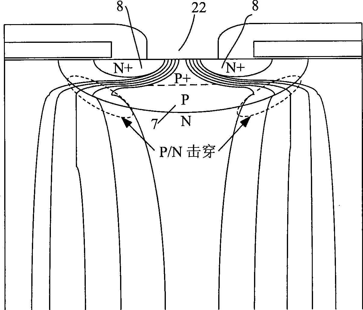
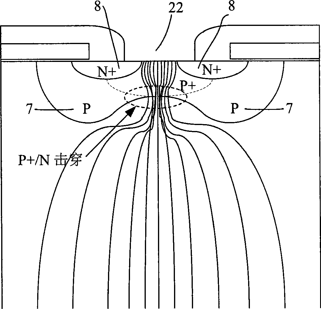
[0023] The present invention proposes an ultra-high density (>5×10 7 Cell / cm 2 ) A new method for realizing the sub-well structure 21 in the design of trench-type power devices effectively solves the contradiction between the realization of the sub-well structure 21 and the ultra-high density design, and is fully compatible with traditional trench-type semiconductor processes and is easy to integrate.

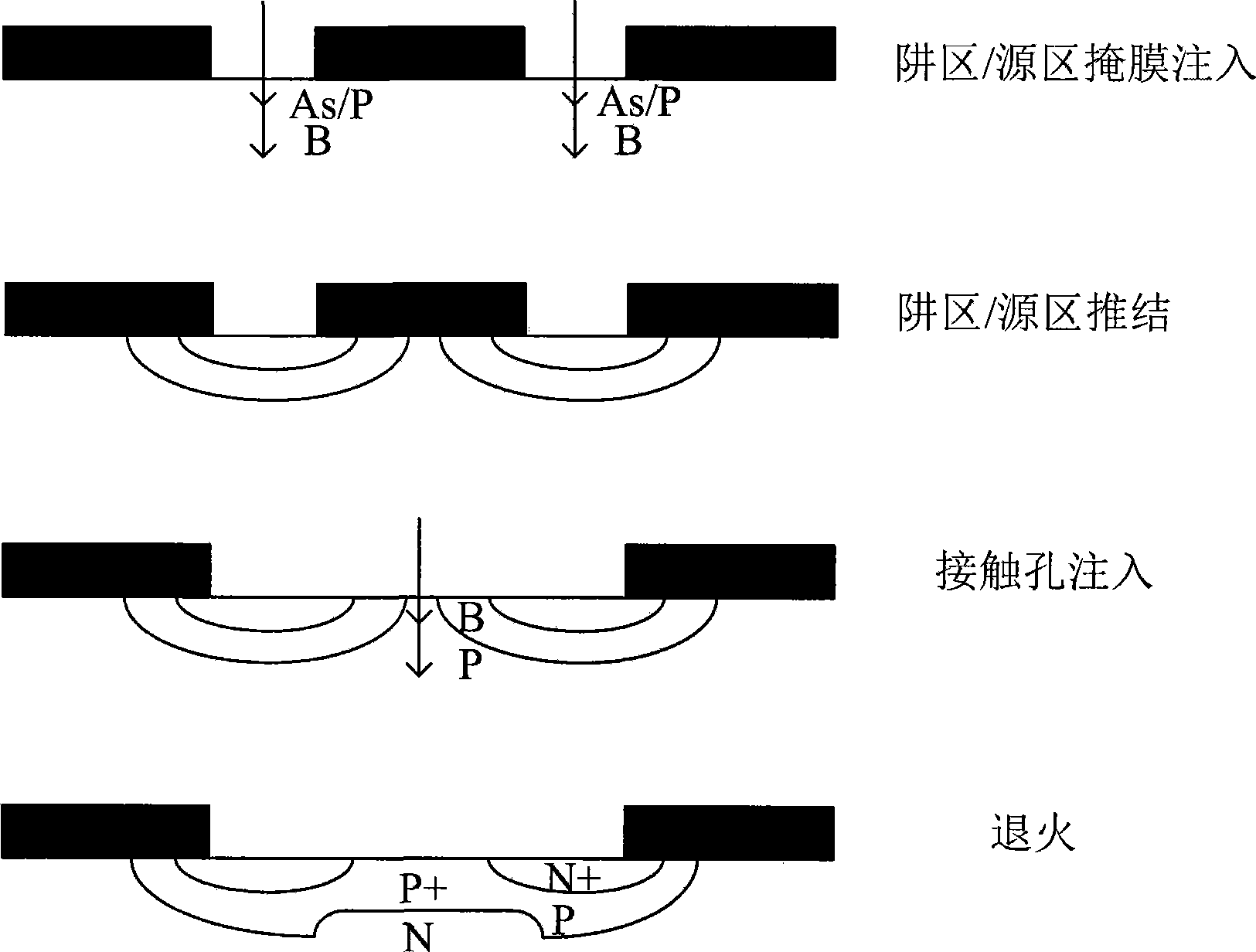
[0024] FIG. 4 describes the key process of implementing the sub-well structure 21 in the design of ultra-high-density trench power devices. Figure 4(a) is trench photolithography, and the photolithographic pattern is transferred to the silicon dioxide 3 / silicon nitride 4 stack as a strong mask for subsequent trench etching; in Figure 4(b), sequentially Trench etching, sacrificial oxide layer, gate oxide layer 5, polycrystalline 6 deposition, and polycrystalline etch-back (Poly Etch-back); in Figure 4(c), well region ion implantation 12, diffusion push junction and Ion implant...


PUM


Abstract

The invention relates to a novel method for achieving a Split Well structure in the design of an ultrahigh-density groove-type power device, and is effective in solving the problem that the Split Well structure (21) is incompatible with the ultrahigh-density design. Based on the impurity compensation theory, the method is characterized in that the high-energy N-type ion injection (18) and the quick annealing are carried out through a contact hole (22) so as to ensure that the Split Well structure (21) is formed at the bottom part in the middle of a well area (7). With the contact hole (22) over-etched below a silicon surface (23), the process ensures that the energy demand for sequential N-type ion injections is effectively reduced, thereby reducing the probability of injection damage to the well area (7) with less leakage sources that cause current to leak out from the device. Moreover, a higher integrated level can be attained with the Split Well structure 21 achieved in Z direction. The novel Split Well technology leads to a substantial improvement on the design of the device which ensures the long-standing reliability of the device as well as the workability of the on-resistance of the device, the firmness of the device and the reverse recovery characteristic of the body diode of the device.

Description

technical field [0001] The present invention relates to a new method for realizing a sub-well structure in a high-density trench type power semiconductor device, in particular to a method for forming a sub-well structure at the bottom of a device well region by using high-energy N-type ion implantation and compensating impurities. A method for realizing a sub-well structure in the Z direction of a device. Background technique [0002] Power semiconductor devices are widely used in computers, network communications, consumer electronics, industrial electronics, automotive electronics, and semiconductor lighting. In recent years, with the expansion of the breadth and depth of semiconductor technology applications, increasing market competition, and the concept of environmental protection and energy saving has become popular, the market has proposed high performance, high reliability, low cost, low power consumption, and miniaturization of power semiconductor devices. higher r...

Claims


Application Information

Patent Timeline
Patent Type & Authority Applications(China)
IPC IPC(8): H01L21/04H01L21/336H01L21/331H01L21/329
Inventor 蒲奎张少锋
Owner 成都方舟微电子有限公司
Why Eureka
Try Eureka