Infrared rapid heat-treatment cavity for semiconductor chip with movable heat baffle

A rapid heat treatment and thermal baffle technology, applied in semiconductor/solid-state device manufacturing, electrical components, circuits, etc., can solve problems such as inability to rapidly cool down, inability to achieve heating and cooling, and inability to accurately control temperature by the temperature control system, achieving high productivity , Wide heating temperature range, fast heating rate and cooling rate

Inactive Publication Date: 2009-04-15
中国电子信息产业集团有限公司 +2
View PDF0 Cites 6 Cited by
  • Summary
  • Abstract
  • Description
  • Claims
  • Application Information

AI Technical Summary

Problems solved by technology

However, annealing semiconductor wafers in the above-mentioned existing heating chamber cannot achieve extremely fast heating and cooling.
Because when the semiconductor chip is sent into the heating chamber, if the temperature rise rate is too fast, due to the thermal inertia of the heater, the preset heating temperature will be greatly exceeded, and the temperature control system cannot accurately control its temperature; When the cavity is heated, the semiconductor chip will continue to be radiated by the heat of the graphite heating cavity and cannot be cooled quickly
Therefore, the infrared rapid heat treatment chamber with the above structure can no longer meet the requirements

Method used


Image

  • Infrared rapid heat-treatment cavity for semiconductor chip with movable heat baffle
  • Infrared rapid heat-treatment cavity for semiconductor chip with movable heat baffle

Examples


Embodiment Construction

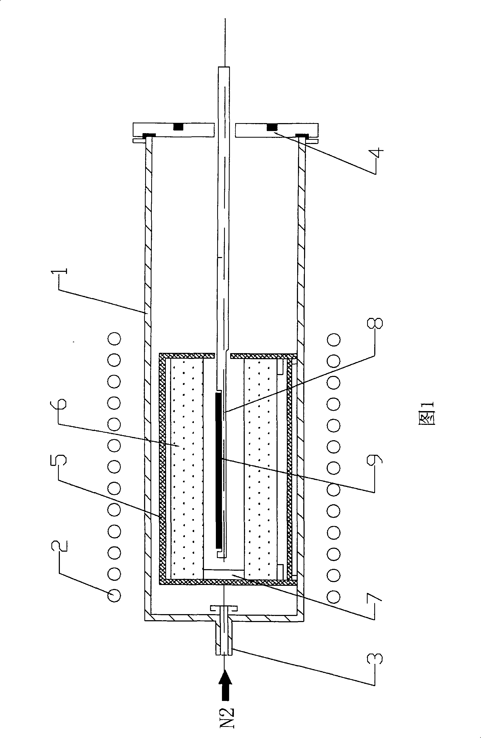
[0010] The infrared rapid heat treatment chamber with movable heat shield semiconductor chip proposed by the present invention is further described as follows in conjunction with the accompanying drawings and embodiments:

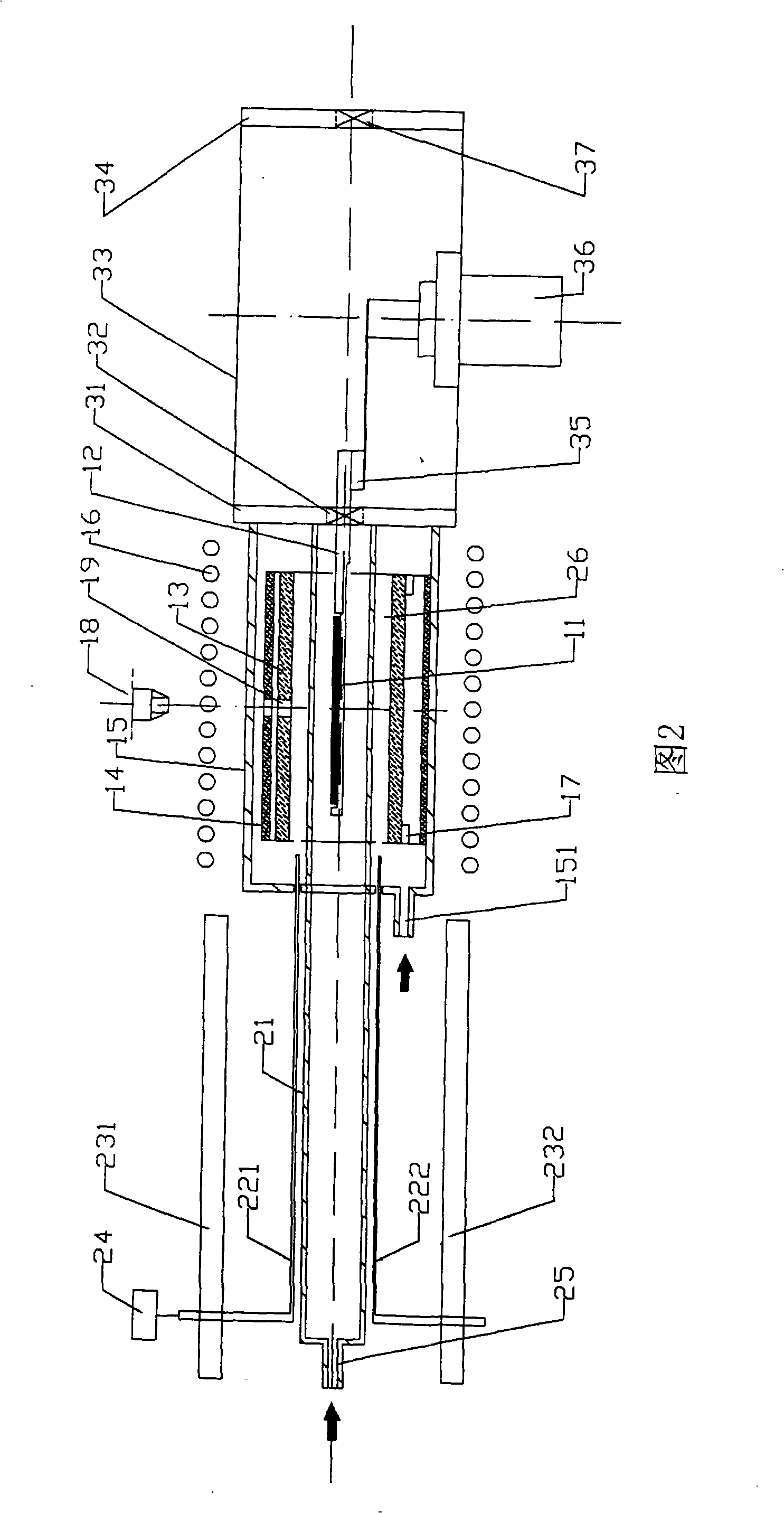
[0011] The overall structure of the embodiment of the infrared rapid heat treatment chamber with movable heat shield semiconductor wafers proposed by the present invention is shown in Figure 2, mainly comprising: a flat rectangle formed by a quartz inner chamber 21 and a quartz outer chamber 15 sleeved outside the inner chamber A double-layer quartz cavity, a flat rectangular graphite heating cavity 13 fixed between the quartz inner cavity and the outer cavity 15 (or adopt graphite material to outsource silicon carbide film, or adopt an infrared heating cavity made of high temperature resistant and oxidation resistant alloy material.) and Infrared reflection plate 14 is wound with radio frequency induction coil 16 outside the quartz outer cavity 15, the oute...


PUM


Abstract

The invention relates to a semiconductor plate infrared fast heat treatment cavity with a movable thermal baffle, belonging to the technical field of the technological device for manufacturing an ultra large scale integrated circuit and a semiconductor. The heat treatment cavity comprises a flat rectangular double-layer quartz cavity, and an infrared heating cavity and an infrared reflection plate which are fixed between an inner quartz cavity and an outer quartz cavity. The front end of the inner quartz cavity extends into the outer quartz cavity. The front ends of the inner quartz cavity and the outer quartz cavity are provided with a sealing cavity cover and a sealing valve thereof. The heat treatment cavity also comprises a mechanical hand which is provided with a quartz plate support fixedly, and a drive mechanism. The movable thermal baffle is also arranged outside the double-layer quartz cavity. The thermal baffle can extend into a gap between the external wall of the inner quartz cavity and the internal wall of a flat rectangular infrared heating cavity from the back end of the double-layer quartz cavity along the direction of axis of the double-layer quartz cavity. The heat treatment cavity of the invention can ensure that a semiconductor plate is heated or cooled fast and realize actual spike annealing. The heat treatment cavity heats the semiconductor plate with uniform temperature within wide range; the heated semiconductor plate has high heating rate and cooling rate; and the semiconductor plate has any size and high production efficiency.

Description

technical field [0001] The invention belongs to the technical field of very large-scale integrated circuits and semiconductor manufacturing process equipment, and in particular relates to the structural design of a semiconductor chip infrared rapid heat treatment chamber. Background technique [0002] In order to meet the requirements of VLSI ultra-shallow junction, silicide formation, thin oxygen growth and rapid thermal nitridation, the inventors of the present application have invented a flat rectangular graphite cavity heated by radio frequency induction as a rapid infrared radiation heat source, so that the infrared The temperature uniformity of the heat treatment quartz chamber of the rapid heat treatment equipment meets the requirements of semiconductor chips below 8″ (Φ200mm) (utility model patent: heat treatment quartz chamber of infrared rapid heat treatment equipment, patent number: 2L 93241758.2). Its structure is shown in Figure 1 A rectangular quartz cavity 1 i...

Claims


Application Information

Patent Timeline
Patent Type & Authority Applications(China)
IPC IPC(8): H01L21/00
Inventor 钱佩信林惠旺刘志弘刘朋刘荣华
Owner 中国电子信息产业集团有限公司
Why Eureka
Try Eureka