

Three-dimensional strain NMOS integrated device and preparation method thereof
An integrated device and three-dimensional technology, which is applied in the field of three-dimensional strained NMOS integrated devices and its production, can solve the problems of low speed of three-dimensional integrated devices, achieve the effects of ensuring AC and DC electrical performance, shortening interconnection lines, and reducing process steps
Inactive Publication Date: 2011-01-05
XIDIAN UNIV
View PDF0 Cites 0 Cited by
- Summary
- Abstract
- Description
- Claims
- Application Information
AI Technical Summary
Problems solved by technology
One of the purposes of the present invention is to provide a three-dimensional strained NMOS integrated device, and the second purpose is to provide a method for manufacturing a three-dimensional strained NMOS integrated device to solve the problem of low speed of existing three-dimensional integrated devices
Method used
View moreImage
Smart ImageViewing Examples

Examples
Embodiment 1
Embodiment 2
Embodiment 3
Login to View More PUM
 Abstract
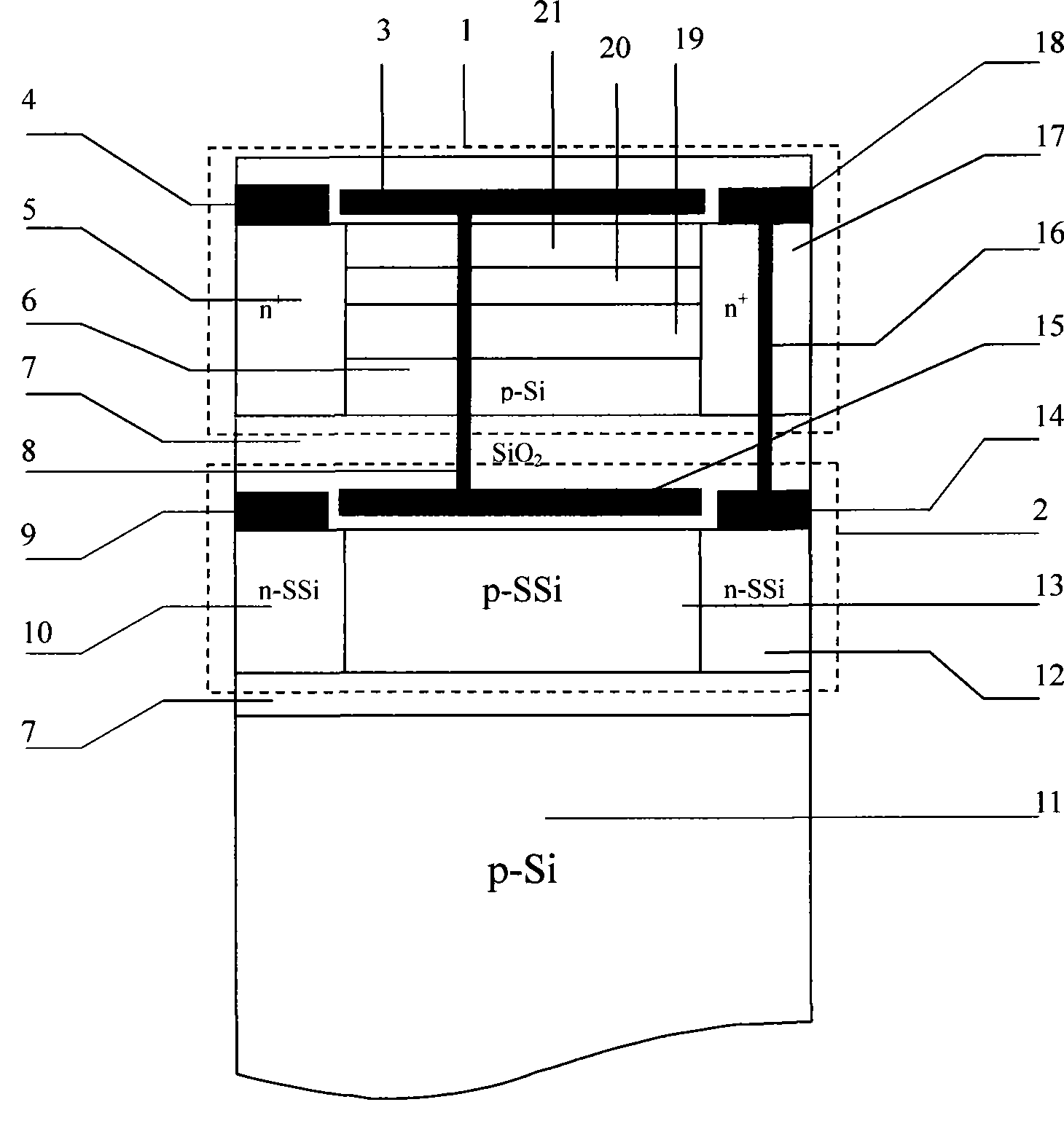
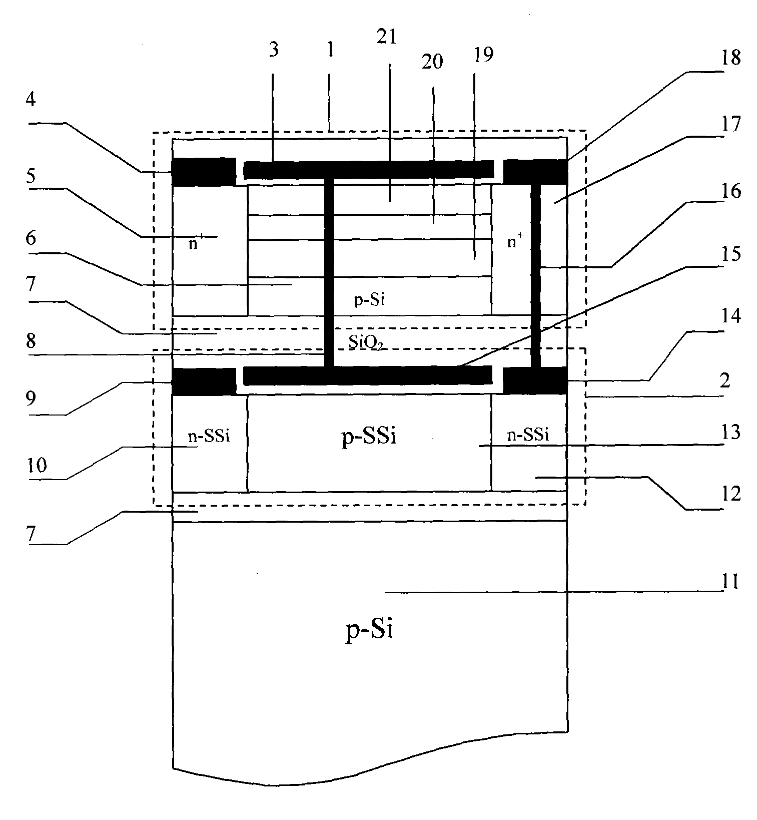
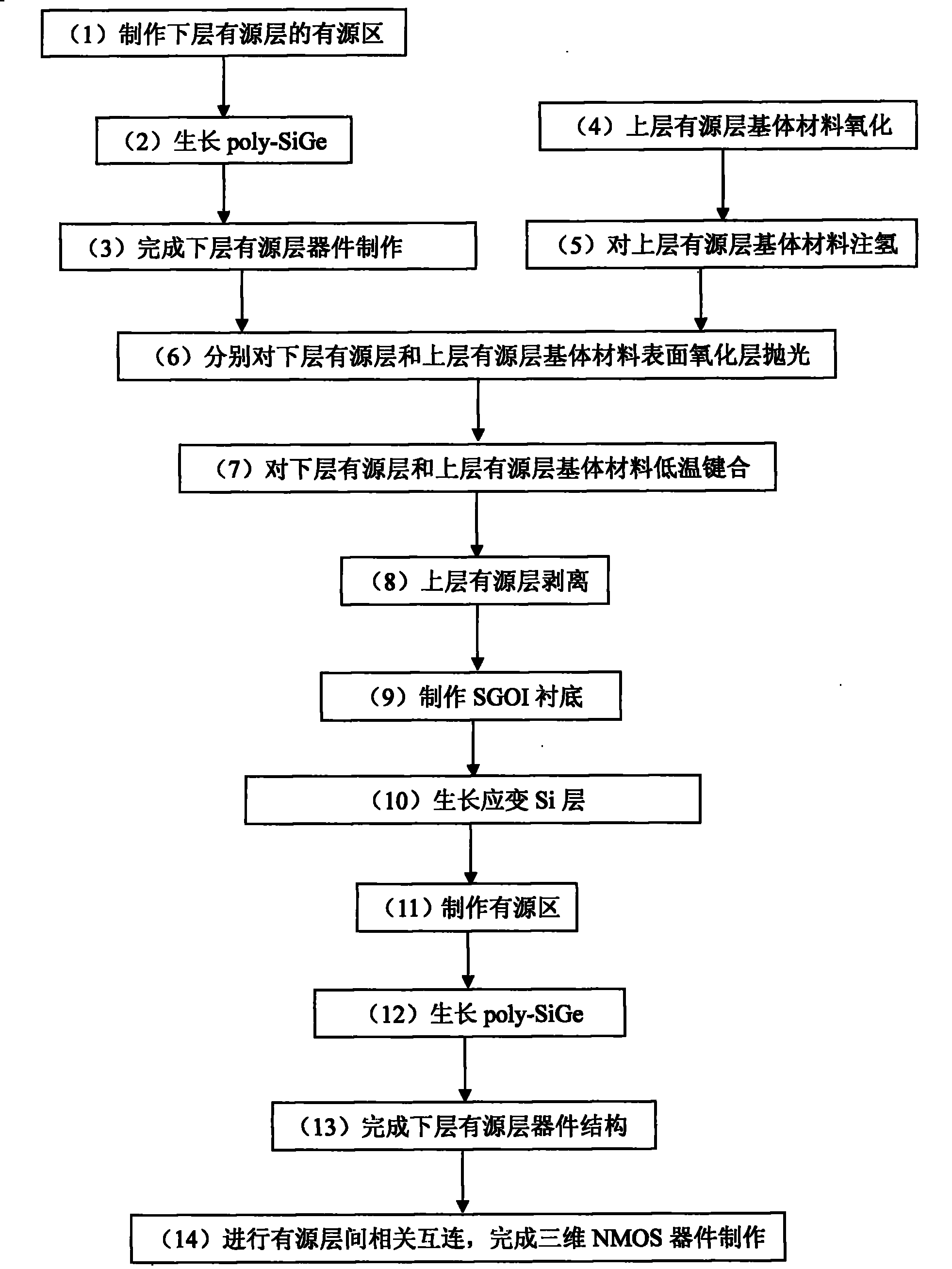
The invention discloses a 3D strained NMOS integrated device and a manufacturing method thereof, relates to the technical field of microelectronics, and mainly solves the problem of low speed of the existing 3D integrated circuit. The proposal is that an SSOI substrate and an SGOI substrate are employed to construct two active layers of a new 3D integrated device; wherein, the lower active layer is the SSOI substrate and is made into strained Si NMOSFET with a poly-SiGe gate by utilizing the characteristic of high electron mobility of a strained Si material in the SSOI substrate; the upper active layer is the SGOI substrate on which a layer of strained Si grows and is made into strained Si surface channel NMOSFET with the poly-SiGe gate; the lower active layer and the upper active layer are connected by an interconnection line to form the 3D strained NMOS integrated device with a conducting channel of 65nm to 130nm. Compared with the existing 3D integrated devices, the 3D strained NMOS integrated device manufactured by the manufacturing method has the advantages of high speed and good performance, and can be applied to manufacturing large-scale and high-speed 3D CMOS integrated circuits.
Description
Three-dimensional strained NMOS integrated device and its fabrication method technical field The invention belongs to the technical field of semiconductor integrated circuits, and in particular relates to a three-dimensional strained NMOS integrated device and a manufacturing method thereof. Background technique Since the 1960s, the feature size of integrated circuits has been continuously reduced following Moore's Law, and the integration and performance of chips have been continuously improved. Entering the deep submicron era, the interconnection of devices inside the chip becomes more and more complex. Therefore, the influence of the delay time caused by the parasitic resistance and parasitic capacitance of the interconnection on the performance of the circuit becomes more and more prominent. Studies have shown that after the feature size of the device is less than 250nm, the R-C delay caused by conventional metal wiring will dominate the entire circuit delay, which re...
Claims
Login to View More Application Information
Patent Timeline
 Patent Type & AuthorityPatents(China)
IPC IPC(8): H01L27/12H01L21/84
Inventor胡辉勇张鹤鸣戴显英宣荣喜宋建军舒斌赵丽霞
OwnerXIDIAN UNIV