Nano-silicon air-sensitive material and gas sensor
A technology of gas-sensitive materials and gas-sensitive elements, which is applied in the field of new material technology and nanomaterials, can solve the problems that it is difficult to achieve ultra-micro-quantity rapid detection, and the sensitivity and selectivity cannot meet the requirements of ultra-micro-quantity rapid detection.
- Summary
- Abstract
- Description
- Claims
- Application Information
AI Technical Summary
Problems solved by technology
Method used
Image

Examples
specific Embodiment approach 2
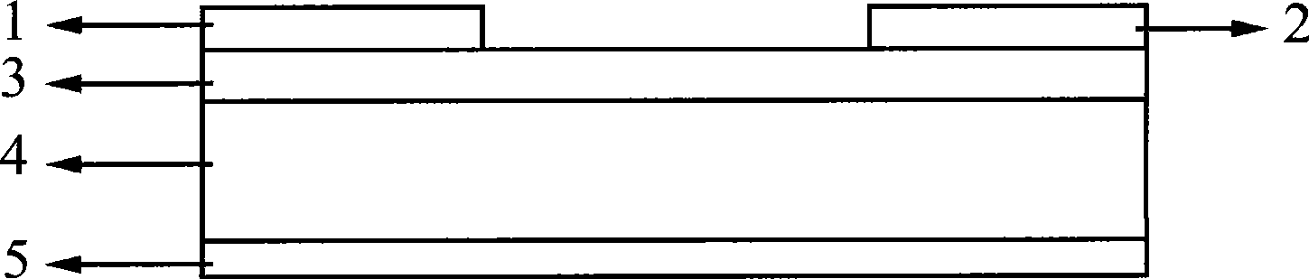
[0028] On the surface of the cleaned silicon chip, deposit a 30nm thick Ag film by electroless plating, then immerse the sample that is deposited with the silver film in a closed container kettle containing hydrofluoric acid and hydrogen peroxide mixed solution (the concentration of hydrofluoric acid and hydrogen peroxide The concentrations are respectively 4.0 mol / L and 0.2 mol / L) and treated for 30 minutes to obtain a large-area nano-silicon material. Metal ohmic electrodes at a certain distance are deposited on the surface of the nano-silicon material, and the outer leads can be drawn out to become a simple gas sensor.
specific Embodiment approach 3
[0029] The cleaned silicon wafer is directly immersed in a closed container kettle containing a mixed solution of hydrofluoric acid and silver nitrate (concentrations of hydrofluoric acid and silver nitrate are respectively 4.0mol / L and 0.02mol / L) and treated for 30 minutes to obtain Large-area nano-silicon material. Metal ohmic electrodes at a certain distance are deposited on the surface of the nano-silicon material, and the outer leads can be drawn out to become a simple gas sensor.
specific Embodiment approach 4
[0030] On the surface of the cleaned silicon chip, deposit a 30nm thick Ag film by electroless plating, then immerse the sample that is deposited with the silver film in a closed container kettle containing hydrofluoric acid and hydrogen peroxide mixed solution (the concentration of hydrofluoric acid and hydrogen peroxide The concentrations are respectively 4.0mol / L and 0.2mol / L) and treated for 40 minutes to obtain a large-area nano-silicon material. Metal ohmic electrodes are deposited on the surface and back of the nano-silicon material, and a simple gas sensor can be formed after the outer lead is drawn out.
PUM
 Abstract
Description
Claims
Application Information
 - R&D Engineer
- R&D Manager
- IP Professional
- Industry Leading Data Capabilities
- Powerful AI technology
- Patent DNA Extraction
Browse by: Latest US Patents, China's latest patents, Technical Efficacy Thesaurus, Application Domain, Technology Topic.
© 2024 PatSnap. All rights reserved.Legal|Privacy policy|Modern Slavery Act Transparency Statement|Sitemap