Circular silicon thin-film solar cell

A technology of solar cells and silicon thin films, applied in circuits, photovoltaic power generation, electrical components, etc., can solve the problems of reducing the photoelectric conversion efficiency of solar cells, reducing the effective power generation area of ​​the battery, and reducing the power generation power of the battery, so as to expand the effective working area, Guaranteed electrical performance and reduced ineffective area

Active Publication Date: 2009-04-29
李毅
View PDF1 Cites 11 Cited by
  • Summary
  • Abstract
  • Description
  • Claims
  • Application Information

AI Technical Summary

Problems solved by technology

However, the patent 200610061259.2 uses a traditional laser as the light source of the laser marking machine, resulting in the laser marking line diameter of the front electrode layer, silicon film layer, and back electrode layer being too large, and the diameter of each laser marking line reaches 0.1 ~0.4mm, according to the structure of the inline silicon thin film solar cell, after the front electrode layer, the silicon thin film layer and the back electrode layer are stacked and connected in series, the width of the invalid area between the battery cells inside the battery can be calculated as: three laser lines The sum of the scribed line diameters is 0.3-1.2mm plus the spacing between the three laser lines and 0.2-0.6mm, that is, the width of the invalid area reaches 0.5-1.8mm, which reduces the effective capacity of the battery to a certain extent. Power generation area, thereby reducing the power generation power of the battery, that is, reducing the photoelectric conversion efficiency of the solar cell

Method used


Image

  • Circular silicon thin-film solar cell
  • Circular silicon thin-film solar cell
  • Circular silicon thin-film solar cell

Examples


Embodiment 1

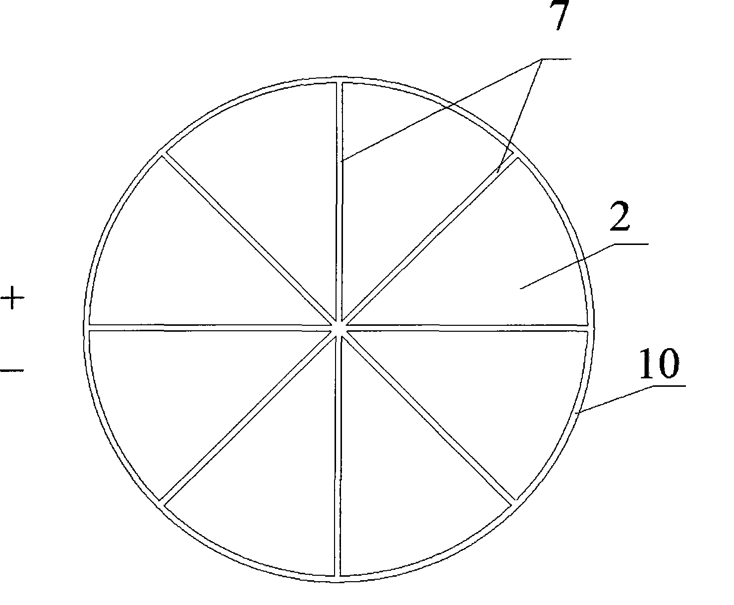
[0037] In this embodiment, the silicon thin film layer 3 is an amorphous silicon thin film, and the circular amorphous silicon thin film solar cell is composed of 8 battery cells connected in series, and the working surface of the battery cells is fan-shaped. Proceed as follows:

[0038] 1. Pattern making of the front electrode layer 2: deposit a layer of transparent ITO conductive film on the transparent substrate 1 to form the front electrode layer 2. Using an end-pumped vibrating mirror infrared laser marking machine, the front electrode layer 2 is etched into fan-shaped independent small blocks with equal areas and mutual insulation to form the laser isolation line 7 of the front electrode layer 2, such as figure 2 shown. The laser wavelength is 1064nm, the laser power is 10 watts, the laser acousto-optic frequency is 40KHz, the width of the laser isolation line 7 on the front electrode layer is 0.07mm, and the insulation resistance between adjacent front electrode patte...

Embodiment 2

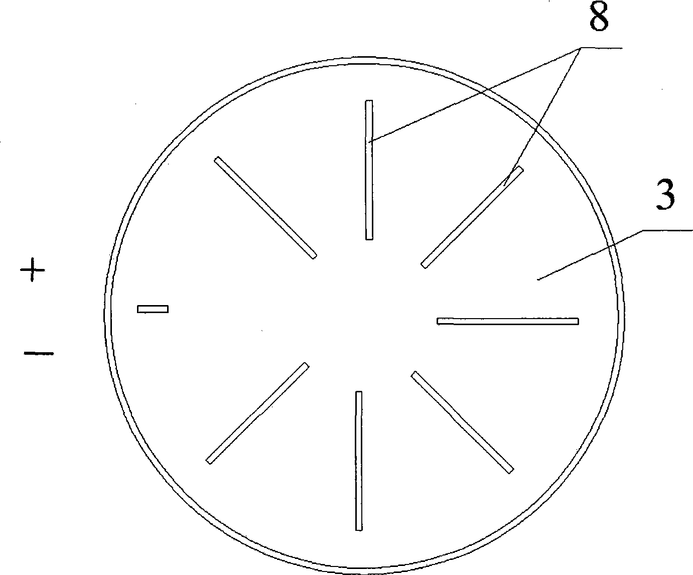
[0047] In this embodiment, the silicon thin film layer 3 is a microcrystalline silicon thin film, and the circular microcrystalline silicon thin film solar cell is composed of 6 battery cells connected in series, and the shape of the battery cells is fan-shaped. Proceed as follows:

[0048] 1. Pattern making of the front electrode layer 2: Deposit a layer of transparent conductive film SnO on the transparent substrate 1 2 , using an end-pumped vibrating mirror infrared laser marking machine to etch the conductive film into fan-shaped independent small pieces with equal areas and mutual insulation. The laser wavelength is 1064nm, the laser power is 20 watts, the laser acousto-optic frequency is 50KHz, the width of the laser isolation line on the front electrode layer is 0.04mm, and the insulation resistance between adjacent front electrode patterns is greater than 20MΩ.

[0049] 2, deposition microcrystalline silicon layer 3: method is the same as embodiment 1, and difference ...

Embodiment 3

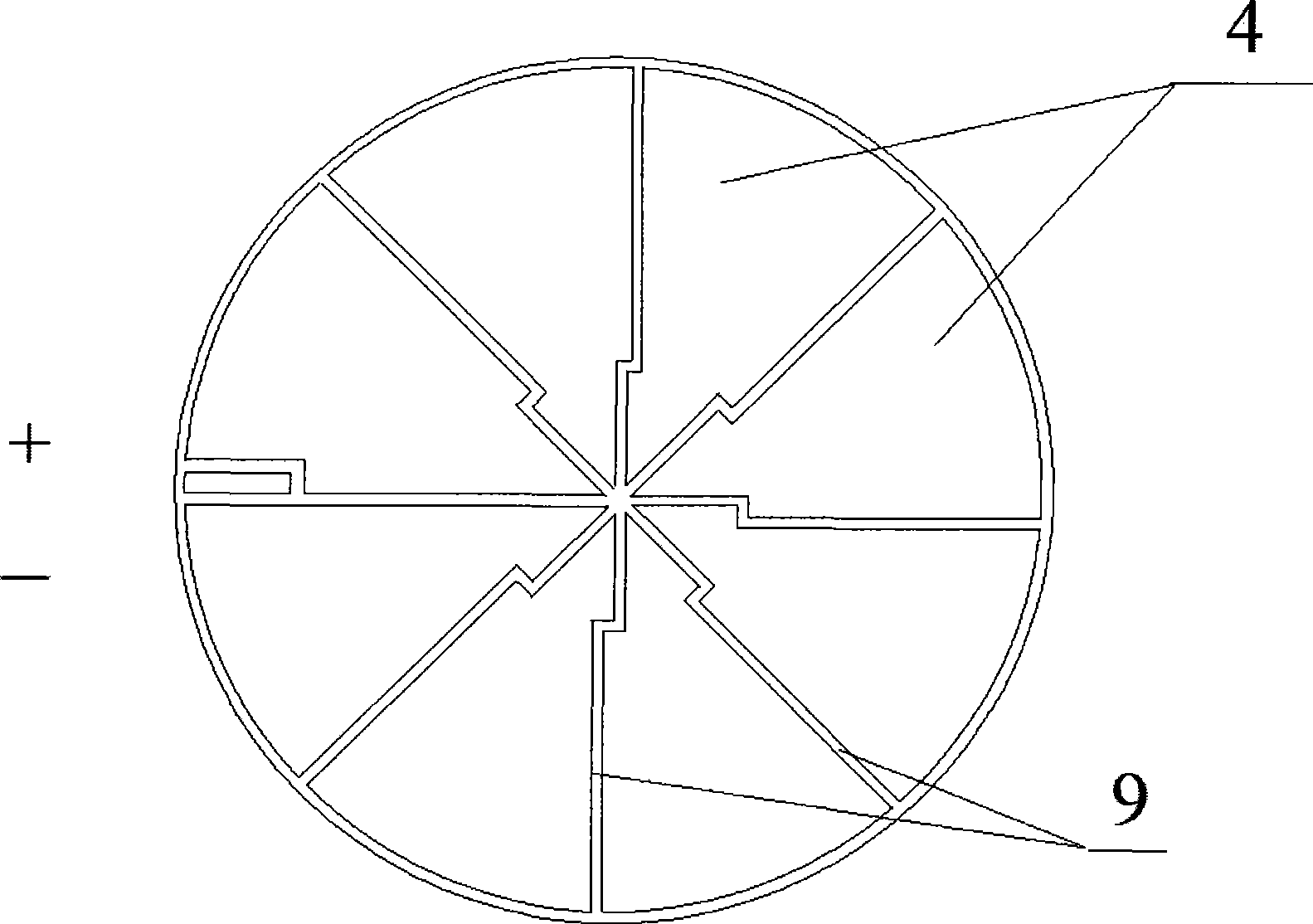
[0055] The silicon thin film layer 3 is an amorphous silicon thin film, and the circular amorphous silicon thin film solar cell is composed of 10 cells with irregular shapes connected in series. Proceed as follows:

[0056] 1. Patterning of the front electrode layer 2: Deposit a layer of transparent SnO on the transparent substrate 1 2 For the conductive film, an end-pumped vibrating mirror infrared laser marking machine is used to etch the conductive film of the front electrode layer into independent small pieces of irregular shape with equal areas. The laser wavelength is 1064nm, the laser power is 29 watts, the laser acousto-optic frequency is 70KHz, the laser isolation line width of the front electrode layer is 0.03mm, and the insulation resistance between adjacent front electrode patterns is greater than 30MΩ.

[0057] 2. Depositing the amorphous silicon thin film layer 3: the method is the same as that in Example 1.

[0058] 3. Laser scribing the amorphous silicon thin...


PUM


Abstract

The invention discloses a round silicon thin film solar cell and a fabrication method thereof. The cell is composed of cell units connected in series, and takes a transparent substrate as a substrate, comprises a front electrode layer, a silicon thin film layer, a back electrode layer and a back paint layer which are stacked up in sequence. The round silicon thin film solar cell is characterized in that working faces of the cell units are formed by laser scribing, an external envelope takes an arc shape, a working face inside the cell is composed of n serially connected cell units which have equal effective area, n is not less than 2, at least two shielding lines and a laser scribing line or a dot-and-dash line which connects a positive electrode and a negative electrode are arranged between the positive electrode and the negative electrode of the cell, and the width between the positive electrode and the negative electrode is 0.03-0.10mm. The fabrication method adopts advanced laser marking technology, can scribe the cell units with fan-shaped or irregular figures, has high precision, and causes the width of an invalid region inside the solar cell to decrease from 0.5-1.8mm to 0.03-0.20mm, thus enlarging the effective working area of the cell.

Description

[0001] Field [0002] The invention discloses a circular silicon thin-film solar cell, which is widely used in various solar electronic instruments and other products, and belongs to the technical field of silicon thin-film solar cells. Background technique [0003] At present, silicon thin-film batteries mainly use amorphous silicon materials. According to different application requirements, solar cells can be made into various shapes. For example, Chinese patent 200610061259.2 "Heterogeneous silicon thin-film solar cells" discloses that the shape and the effective working surface of the battery are complex and diverse. Special-shaped solar cells can also be made into transparent windows of various shapes by drilling holes or laser scribing in the cell surface. However, the patent 200610061259.2 uses a traditional laser as the light source of the laser marking machine, resulting in the laser marking line diameter of the front electrode layer, silicon film layer, and back ele...

Claims


Application Information

Patent Timeline
Patent Type & Authority Applications(China)
IPC IPC(8): H01L31/042
CPCY02E10/50
Inventor 李毅李全相胡盛明
Owner 李毅
Why Eureka
Try Eureka