Gallium nitride base LED chip and preparation method thereof

A light-emitting diode, gallium nitride-based technology, applied in the direction of electrical components, circuits, semiconductor devices, etc., can solve the problems of reducing the total reflection of the light-emitting diode chip, low luminous efficiency outside the light-emitting diode chip, and increasing the extraction of side light. Achieve the effects of increasing light extraction efficiency, improving external luminous efficiency, and reducing total reflection

Inactive Publication Date: 2009-05-20
ZHEJIANG INVENLUX TECH
View PDF0 Cites 25 Cited by
  • Summary
  • Abstract
  • Description
  • Claims
  • Application Information

AI Technical Summary

Problems solved by technology

[0004] In view of this, in order to solve the problem of low external luminous efficiency of gallium nitride-based light-emitting diode chips in the prior art, the main purpose of the present invention is to provide a gallium nitride-based l

Method used


Image

  • Gallium nitride base LED chip and preparation method thereof
  • Gallium nitride base LED chip and preparation method thereof
  • Gallium nitride base LED chip and preparation method thereof

Examples


Embodiment 1

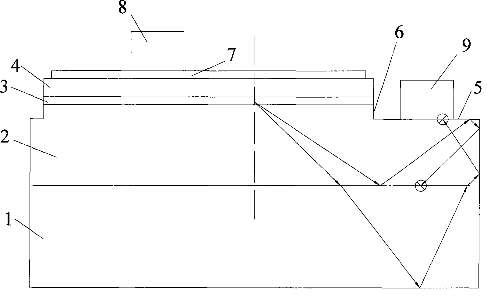
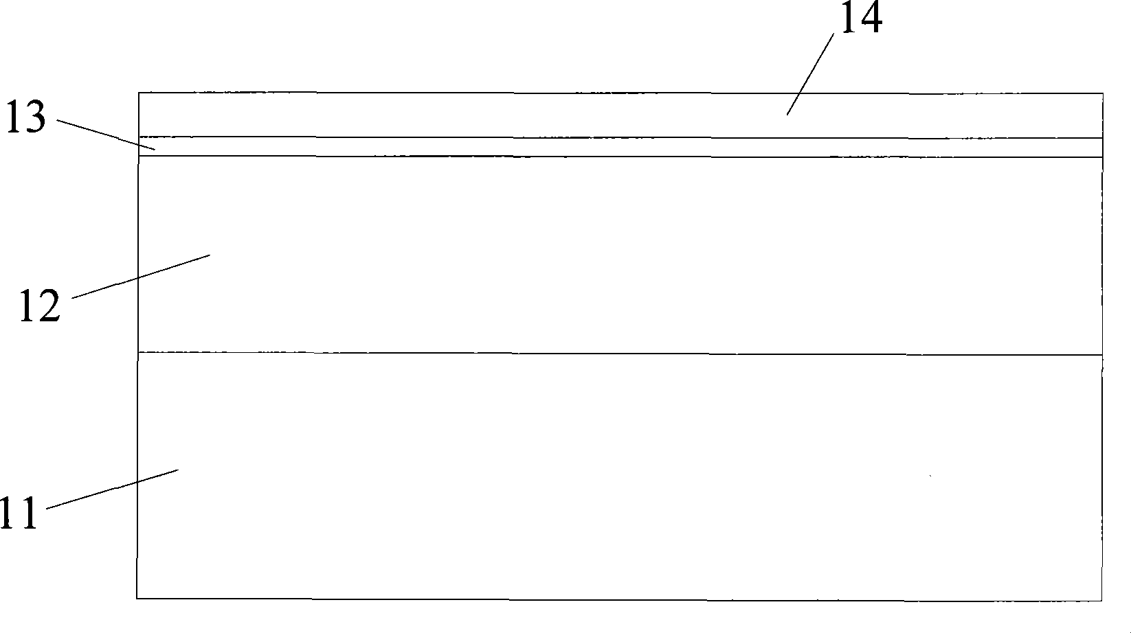
[0033] Provide a GaN-based light-emitting diode epitaxial wafer, such as figure 2 As shown, the structure of the epitaxial wafer includes a sapphire substrate II, an N-type GaN layer 12 , an active layer 13 , and a P-type GaN layer 14 . Besides sapphire, the material of the substrate can also be silicon carbide, zinc sulfide or gallium arsenide.

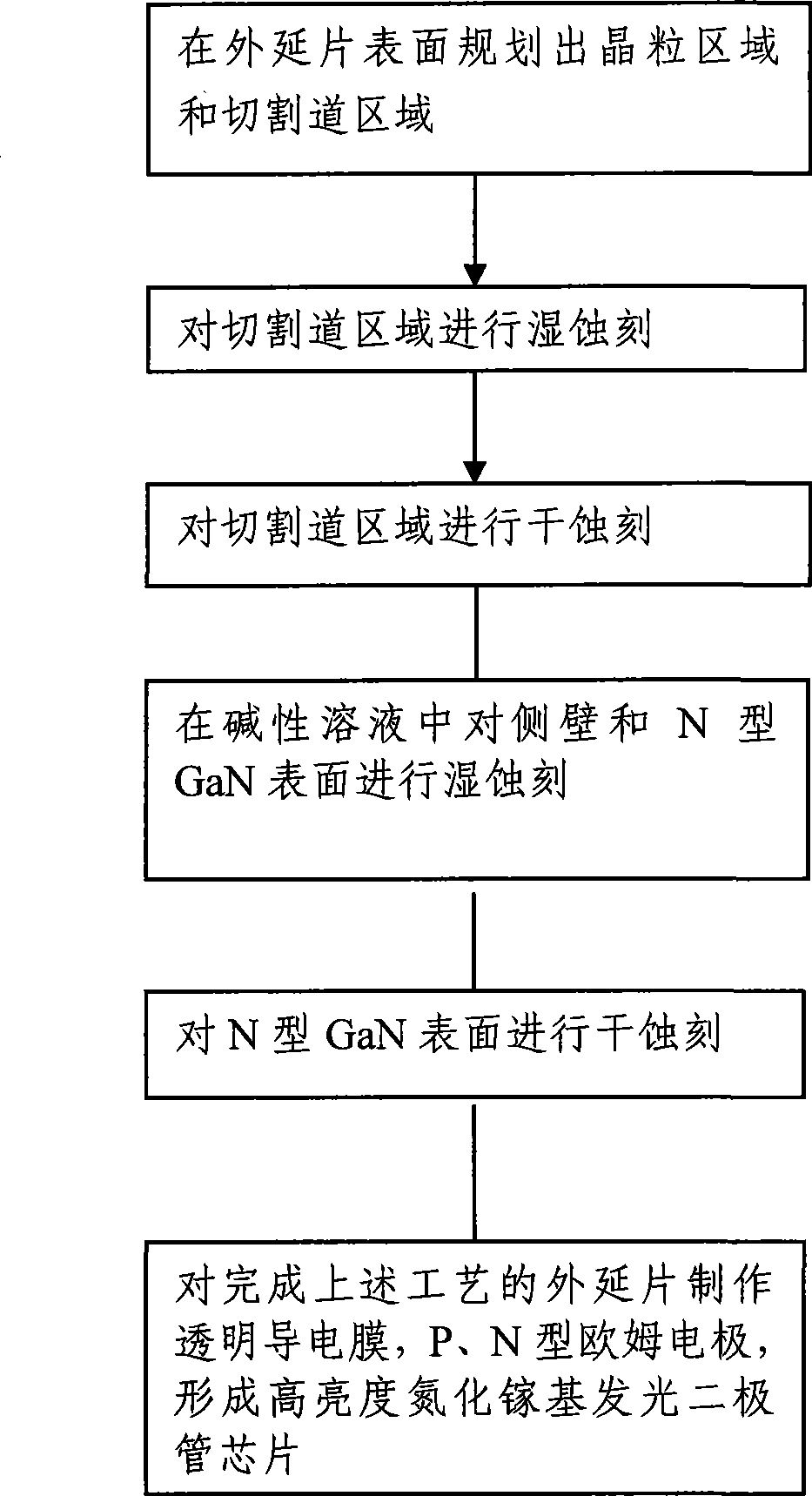
[0034] Please refer to image 3 , the manufacturing method of gallium nitride-based light-emitting diode chip described in the present invention, comprises the following steps:

[0035] (1) First generate a protective mask 15 on the surface of the epitaxial wafer, then coat photoresist, then use a photolithography mask to photoetch and develop on the photoresist surface, plan the pattern of the grain area and the pattern of the scribe line area 16 graphics,

[0036] (2) Carry out wet etching to the scribe line region 16, etch and remove the protection mask 15 of the scribe line region 16, finally remove the undeveloped photoresis...

Embodiment 2

[0042] The manufacturing method of the gallium nitride-based light-emitting diode chip according to the present invention comprises the following steps:

[0043] (1) First generate a protective mask 15 on the surface of the epitaxial wafer, then coat photoresist, then use a photolithography mask to photoetch and develop on the photoresist surface, plan the pattern of the grain area and the pattern of the scribe line area 16 graphics,

[0044](2) Carry out wet etching to the scribe line area 16, etch and remove the protective mask 15 of the scribe line area 16, finally remove the undeveloped photoresist, and expose the protective mask 15 on the grain area surface,

[0045] (3) Under a pressure environment of 10 millitorr, use a plasma etching machine to dry-etch the scribe line region 16 mainly by chemical etching, expose the N-type GaN layer 12 and form sidewalls, and the N-type GaN layer 12 after dry etching The distance between the surface 18 of the type GaN and the surface...

Embodiment 3

[0050] The manufacturing method of the gallium nitride-based light-emitting diode chip according to the present invention comprises the following steps:

[0051] (1) First generate a protective mask 15 on the surface of the epitaxial wafer, then coat photoresist, then use a photolithography mask to photoetch and develop on the photoresist surface, plan the pattern of the grain area and the pattern of the scribe line area 16 graphics,

[0052] (2) Carry out wet etching to the scribe line area 16, etch and remove the protective mask 15 of the scribe line area 16, finally remove the undeveloped photoresist, and expose the protective mask 15 on the grain area surface,

[0053] (3) Under the pressure environment of 7 mTorr, use the plasma etching machine to dry-etch the scribe line region 16 mainly by chemical etching, expose the N-type GaN layer 12 and form sidewalls, and the N-type GaN layer 12 after dry etching The distance between the GaN surface 18 and the surface of the sapp...


PUM

PropertyMeasurementUnit
Depthaaaaaaaaaa
Roughnessaaaaaaaaaa
Roughnessaaaaaaaaaa

Abstract

The invention relates to a gallium nitride based light-emitting diode chip and a method for manufacturing the same. The method comprises the following steps: planning a crystal grain area and a cutting path area on the surface of an epitaxial slice; removing a protective mask of the cutting path area and then removing an undeveloped photoresist; performing dry etching on the cutting path area to expose N-type gallium nitride and form a side wall, wherein the distance between the surface of the N-type gallium nitride and the surface of a substrate of the epitaxial slice is between 1 and 1.5mu m; performing wet etching on the side wall and the surface of the N-type gallium nitride in an alkaline solution so as to form a roughened side wall of the N-type gallium nitride and a roughened surface of the N-type gallium nitride; and performing dry etching on the surface of the N-type gallium nitride, making use of the lattice defect formed in the process of epitaxy to form a nanometer columnar structure on the surface of the N-type gallium nitride, and finally manufacturing the chip. The chip can improve the external luminous efficiency of the gallium nitride based light-emitting diode chip.

Description

technical field [0001] The invention belongs to the technical field of gallium nitride-based light-emitting diodes, and in particular relates to a gallium nitride-based light-emitting diode chip and a manufacturing method thereof. Background technique [0002] Semiconductor light-emitting diodes are increasingly widely used, especially in the trend of replacing incandescent and fluorescent lamps in lighting, but there are still some technical problems, especially the low light extraction efficiency. Usually, there are three main reasons for affecting the light extraction efficiency. : One is due to the absorption of light by the material, the other is the total reflection of light when passing through different media, and the other is the loss of light due to the Fresnel effect. [0003] At present, the conventional technology for manufacturing light-emitting diode chips is to sequentially grow epitaxial growth on the substrate 1 to obtain the structure of the light-emitting...

Claims


Application Information

Patent Timeline
IPC IPC(8): H01L33/00H01L33/22
Inventor 陈国聪王孟源陆前军
Owner ZHEJIANG INVENLUX TECH
Why Eureka
Try Eureka