Integrated micro-mechanical thermopile infrared detection system and method for producing the same

A thermopile detector and infrared detection technology, applied in the field of infrared detectors, can solve problems such as difficult mass production and large device size

Inactive Publication Date: 2009-07-08
SHANGHAI INST OF MICROSYSTEM & INFORMATION TECH CHINESE ACAD OF SCI
View PDF0 Cites 19 Cited by
  • Summary
  • Abstract
  • Description
  • Claims
  • Application Information

AI Technical Summary

Problems solved by technology
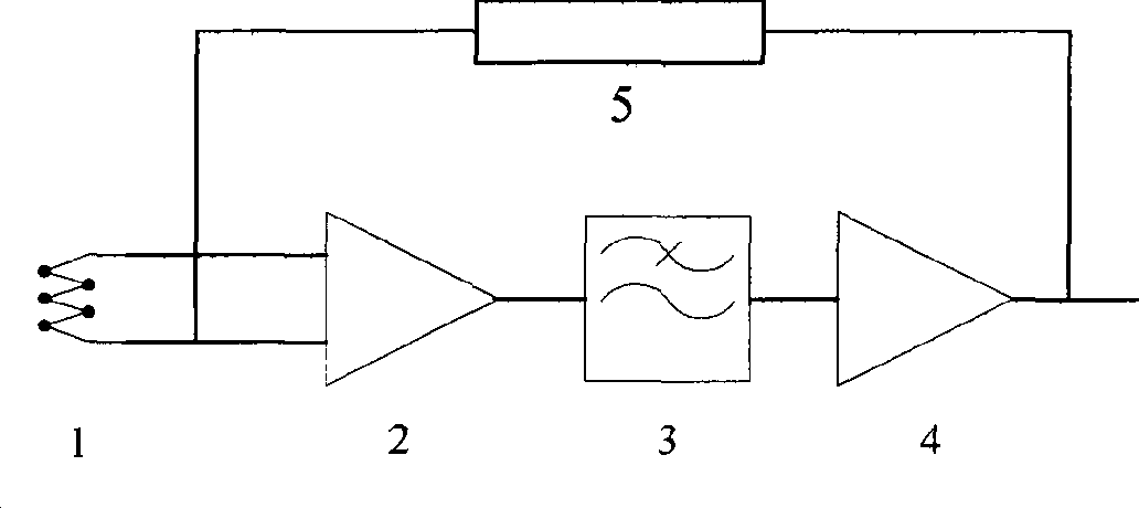
Early thermopile infrared detectors were obtained by depositing thermocouple materials on plastic or alumina substrates by vacuum coating. The device size is large and it is not easy to mass produce.

Method used


Image

  • Integrated micro-mechanical thermopile infrared detection system and method for producing the same
  • Integrated micro-mechanical thermopile infrared detection system and method for producing the same
  • Integrated micro-mechanical thermopile infrared detection system and method for producing the same

Examples


Embodiment 1

[0058] The main process steps include:

[0059] (1) Select a P+ silicon wafer (not shown in the figure) with a (100) crystal orientation as the substrate, with a resistivity of 10 Ω cm, and initially oxidize the P- epitaxial layer 14 to grow silicon oxide

[0060] (2) Lithograph the N well 16 on the P- epitaxial layer, ion implant phosphorus, and dose 2E12cm -2 , the energy is 60keV, the well region is advanced, and the junction depth is about 6.0μm.

[0061] (3) Growth of thermal silicon oxide LPCVD deposition thickness is of silicon nitride 17.

[0062] (4) Photoetching the active area of ​​the CMOS circuit, etching silicon nitride and silicon oxide.

[0063] (5) Etch the silicon wafer and grow about The field oxide layer 18.

[0064] (6) Etching and removing silicon nitride and silicon oxide in the CMOS circuit area.

[0065] (7) The growth thickness of the active region is about The gate oxide layer 19.

[0066] (8) LPCVD deposits polysilicon 20 with a thickne...

Embodiment 2

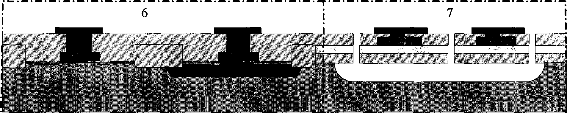
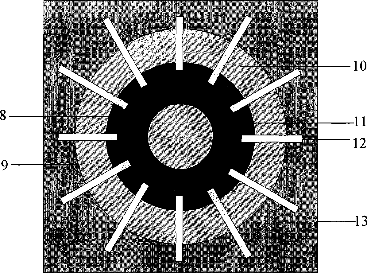
[0075] Its specific implementation steps are the same as in Example 1, the main difference is that the thermopile geometric configuration in Example 1 is modified to Figure 5 in the structure. The geometry of the thermocouple pair is not image 3 Shown are radial rather than parallel to the sides of the frame; etch openings are designed to be square rather than image 3 Circular shapes are shown, no special crystallographic orientations need to be considered.

Embodiment 3

[0077] The specific implementation steps are the same as those in Embodiment 1, the main difference being that the N-well CMOS process in Embodiment 1 is modified to a P-well or double-well CMOS process. Taking the P-well CMOS process as an example, the modified process steps are as follows: (a) Change the P+ silicon wafer in step (1) in Embodiment 1 to an N+ silicon wafer as the substrate. (b) Modify step (2) in Example 1 to "photolithographically P-well on the N- epitaxial layer, and ion-implant boron with a dose of 5E12cm -2 , the energy is 60keV, the well region advances, and the junction depth is about 6.0μm". (c) "Ion implantation of boron in step (8) in Example 1, the dose is 5E15cm -2 , the energy is 80keV" is modified to "ion implantation of phosphorus, the dose is 5E15cm -2 , the energy is 60keV". (d) Ion-implant boron 22 into the "PMOS region" in step (9) of Example 1, with a dose of 8E15cm -2 , the energy is 60keV" is changed to "Ion implantation of phosphorus in...


PUM

PropertyMeasurementUnit
electrical resistivityaaaaaaaaaa

Abstract

The invention provides an integrated micromechanical thermopile infrared detection system and a manufacture method thereof. The system comprises a thermopile detector and a signal processing circuit, wherein the signal processing circuit comprises a preposed amplifier, a band-pass filter, a main amplifier and an oscillator. The method is characterized in that integrated design and manufacture of a uniwafer of the thermopile detector and the signal processing circuit are realized; and compatibility of a MEMS sensor and a CMOS circuit can be realized by manufacturing the thermopile detector and the signal processing circuit simultaneously and using a standard CMOS process. The structure of the thermopile detector in the system comprises a (silicon) matrix, a framework, a thermoelectric couple, a support arm, an infrared absorption layer, etching openings; and the intermediate suspended infrared absorption layer can be provided with the etching openings with different shapes, and dry etching working gas enters a substrate etched silicon releasing structure through the etching openings. The structure of the signal processing circuit in the system uses wave chopping technology to reduce the effect of low-frequency noise on a signal.

Description

technical field [0001] The present invention relates to an integrated micromechanical thermopile infrared detection system and a manufacturing method thereof, more precisely the present invention relates to a micromechanical thermopile infrared detection system based on a MEMS (Micro-Electro-Mechanical System) sensor and a CMOS signal processing circuit The system and its manufacturing method belong to the field of infrared detectors. Background technique [0002] With the increasing status of infrared detection technology in military and civilian fields, uncooled infrared sensors are developing rapidly. The thermopile infrared detector is the earliest developed thermal infrared detector, and its working principle is the Seebeck effect [T.H.Geballe and G.W.Hull, "Seebeck Effect in Silicon," Phys.Rev., vol.98, No.4, pp. 940-947, May 1955.]. This effect states that for a thermocouple composed of two dissimilar materials, if there is a temperature difference between the two n...

Claims


Application Information

Patent Timeline
Patent Type & Authority Applications(China)
IPC IPC(8): G01J5/14B81B7/02B81C1/00
Inventor 熊斌杨恒昭徐德辉刘米丰王跃林
Owner SHANGHAI INST OF MICROSYSTEM & INFORMATION TECH CHINESE ACAD OF SCI
Why Eureka
Try Eureka