
System and method for validating and testing on-chip system

A system-on-chip and test interface technology, which is applied in the computer field, can solve problems such as slow speed, and achieve the effect of reducing the delay of pins, improving the speed of verification, and increasing the speed

Inactive Publication Date: 2009-08-12
ACTIONS ZHUHAI TECH CO
View PDF0 Cites 26 Cited by
  • Summary
  • Abstract
  • Description
  • Claims
  • Application Information

AI Technical Summary

Problems solved by technology

[0008] The purpose of the embodiments of the present invention is to provide a system for verifying a system-on-chip to solve the problems of slow speed and the need for a large number of pins when verifying a system-on-chip in the prior art

Method used


Image

  • System and method for validating and testing on-chip system
  • System and method for validating and testing on-chip system
  • System and method for validating and testing on-chip system

Examples


Embodiment 1

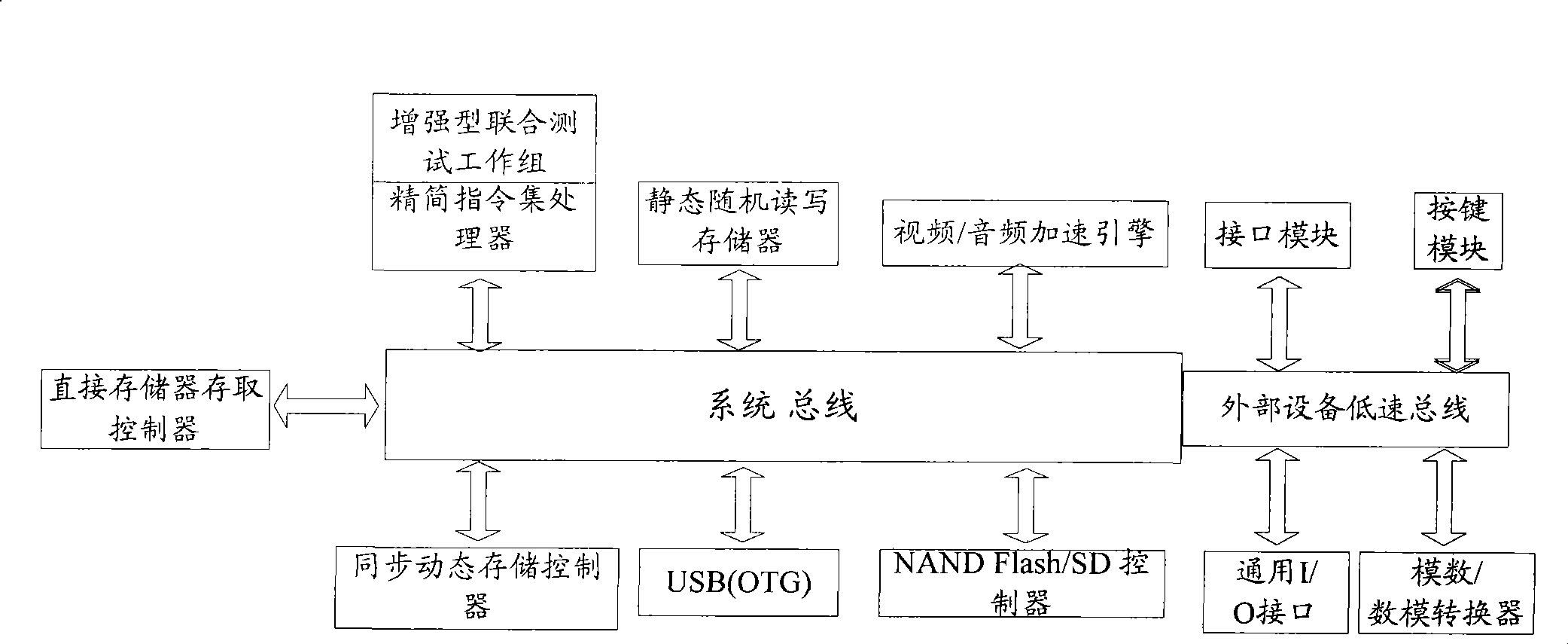
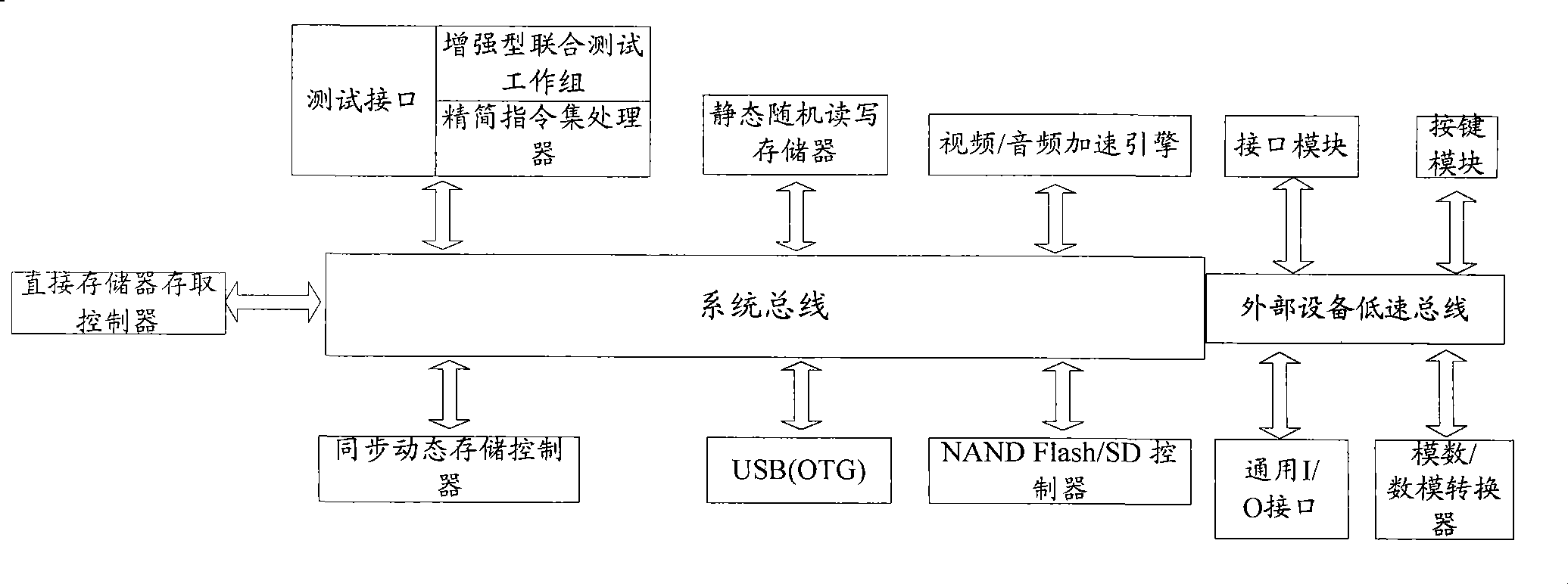
[0077] Implementation 1: The verification stimulus device only includes the RISP bus control unit, so that the system-on-chip needs to be verified only through the test interface circuit, the data connected between the test interface circuit and the RISC bus control unit, and the control line interface is The first interface, the specific process is as follows, see Image 6 :

[0078] Step 601: Determine that the operating mode of the SoC emulation device is the first operating mode, and at this time, the test interface circuit controls the system bus mode.

[0079] By injecting the clock signal, the reset signal and the timing of the mode signal, the system-on-chip emulation device runs in the first working mode.

[0080]Step 602: The reduced instruction set processor bus control unit sends verification programs to the test interface circuit through the first interface. These verification programs include parsing the assembly-like instruction set to generate verification tim...

Embodiment 2

[0086] Embodiment 2: According to the architecture of the above system-on-chip verification, the verification stimulus device includes an RISP bus control unit and an enhanced joint test working group bus control unit. For data between the test interface circuit in the simulation device and the RISP bus control unit, the control line interface is the first interface, between the RISC processor in the simulation device and the enhanced joint test working group bus control unit The data of the control line interface is an enhanced joint test working group interface. The specific process of system-on-chip verification is as follows, see Figure 7 :

[0087] Step 701: Determine that the working mode of the SoC is the first working mode, and at this time, the test interface circuit controls the state of the system bus.

[0088] In the embodiment of the present invention, by controlling the pins of the SOC simulation device, that is, by injecting the clock signal, the timing sequen...

Embodiment 3

[0128] Implementation 3: The test stimulus device only includes the RISP bus control unit, so that the system-on-chip needs to be tested only through the test interface circuit, the data connected between the test interface circuit and the RISC bus control unit, and the control line interface is The first interface, the specific process is as follows, see Figure 11 :

[0129] Step 1101: Determine that the working mode of the system on chip is the first working mode, and at this time, the test interface circuit controls the system bus mode.

[0130] The system-on-chip runs in the first working mode by pouring in the timing of the clock signal, the reset signal and the mode signal.

[0131] Step 1102: The RISP bus control unit simulates the test timing signal according to the test vector generated in the verification process. Here, the verification process can be performed according to the verification method provided in the embodiment of the present invention, or according t...


PUM


Abstract

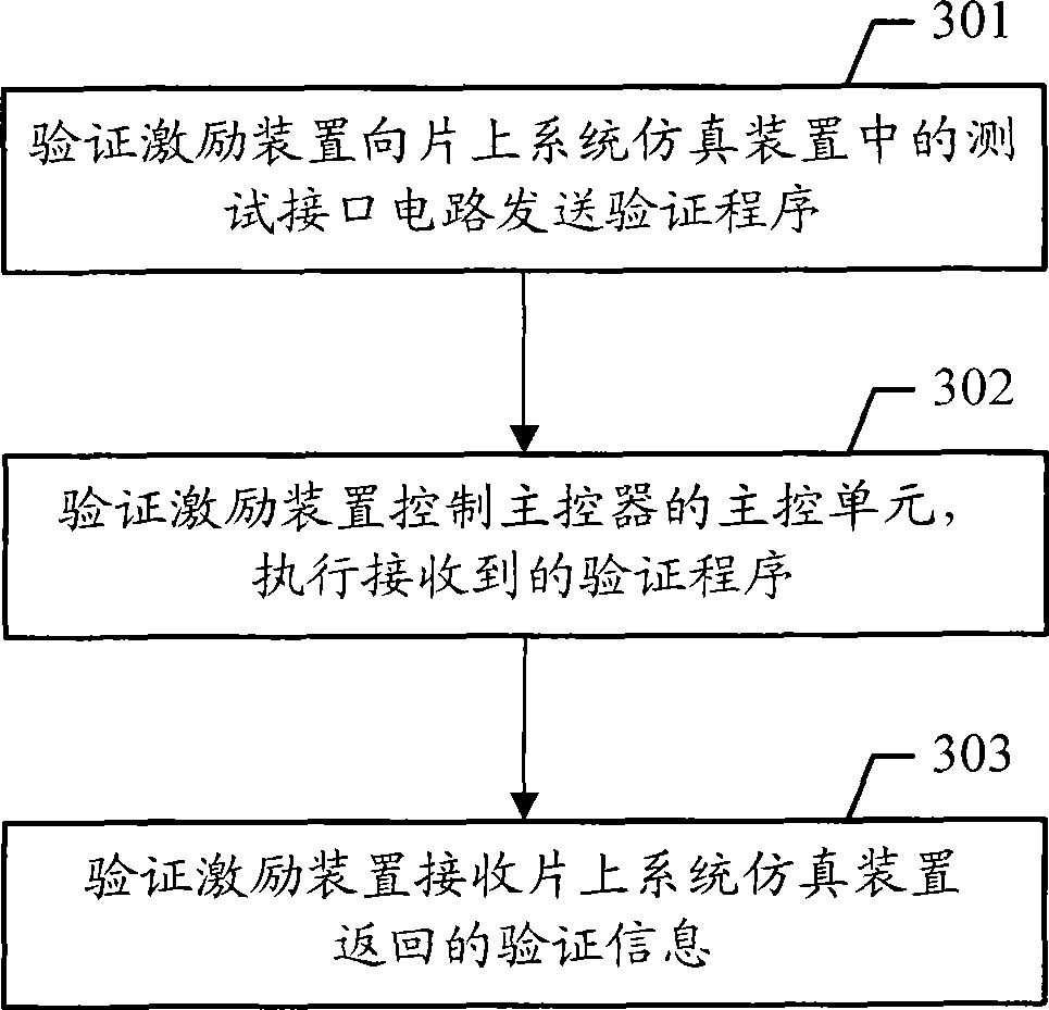
The invention discloses a system for verifying a system on a chip (SoC), which is used for solving the problems of low speed and requirement of a large number of pins when the SoC is verified in the prior art. The system comprises a verification exciting device and an SoC simulation device, wherein the verification exciting device is connected with a test interface circuit in the SoC simulation device and used for transmitting a verification program to the test interface circuit, driving the SoC simulation device to execute the received verification program, and receiving verification information returned by the SoC simulation device; and the SoC simulation device is used for receiving the verification program, executing the received verification program under the driving of the verification exciting device, and returning the verification information to the verification exciting device. The invention also discloses a method for verifying the SoC and a system and a method for verifying the SoC.

Description

technical field [0001] The invention relates to the field of computer technology, in particular to a system and method for verifying and testing a system on a chip. Background technique [0002] System on a Chip (SoC, System on a Chip) is a system that integrates microprocessors, analog IP cores, digital IP cores, and memory or off-chip storage control interfaces on a single chip. Standard product for the purpose. [0003] The system-on-chip configuration can include: system-on-chip control logic module, microprocessor / microcontroller core module, digital signal processor module, embedded memory module, interface module for communicating with the outside, and analog front-end including analog / digital / digital-analog Modules, power supply and power management modules, etc. For a wireless system-on-chip, there are also RF front-end modules, user-defined logic, and micro-electromechanical modules. More importantly, a system-on-chip chip is embedded with basic software modules o...

Claims


Application Information

Patent Timeline
Patent Type & Authority Applications(China)
IPC IPC(8): G06F17/50
Inventor 张奇
Owner ACTIONS ZHUHAI TECH CO
Learn More