AlGaN-based multiple quantum well uv-LED device based on SiC substrate and manufacturing method

A quantum well and device technology, applied in semiconductor devices, electrical components, circuits, etc., can solve the problems of high turn-on voltage, long exit path, and only 0.01% external quantum efficiency, so as to increase output power, increase exit power, The effect of promoting the practical process

Inactive Publication Date: 2009-08-26
XIDIAN UNIV
View PDF0 Cites 22 Cited by
  • Summary
  • Abstract
  • Description
  • Claims
  • Application Information

AI Technical Summary

Problems solved by technology

In 2004, a 250nm LED was produced. The maximum power of a 200μ×200μ chip is close to 0.6mW, but the external quantum efficiency is only 0.01%.
As the emission wavelength decreases, the bottom buffer layer absorbs more and more ultraviolet light, which seriously affects the output light power and external quantum efficiency.
The existing technology of emitting light from the bottom still has great shortcomings. First, the light emission path is too long, and the loss of light in the middle is too large, often resulting in low external quantum efficiency of light; second, the crystal quality of the bottom AlN buffer layer is low. Poor, resulting in an increase in the non-radiative recombination center of the material, and more absorption of ultraviolet light; third, the shape of the p-type electrode is more complicated, and often requires higher process requirements, which brings a lot of problems to the repeatability of this process. problem
Fourth, the complex electrode structure results in a higher turn-on voltage

Method used


Image

  • AlGaN-based multiple quantum well uv-LED device based on SiC substrate and manufacturing method
  • AlGaN-based multiple quantum well uv-LED device based on SiC substrate and manufacturing method

Examples


Embodiment 1

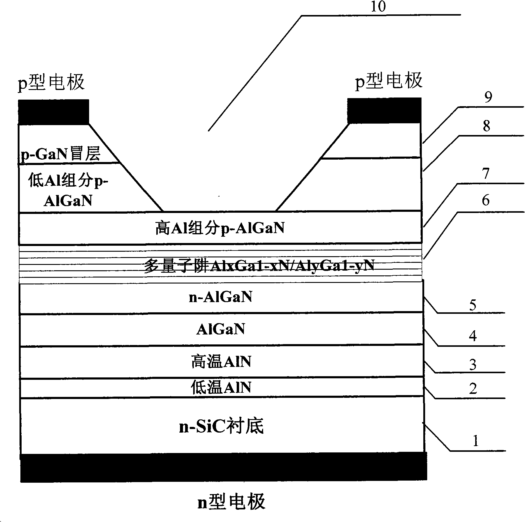
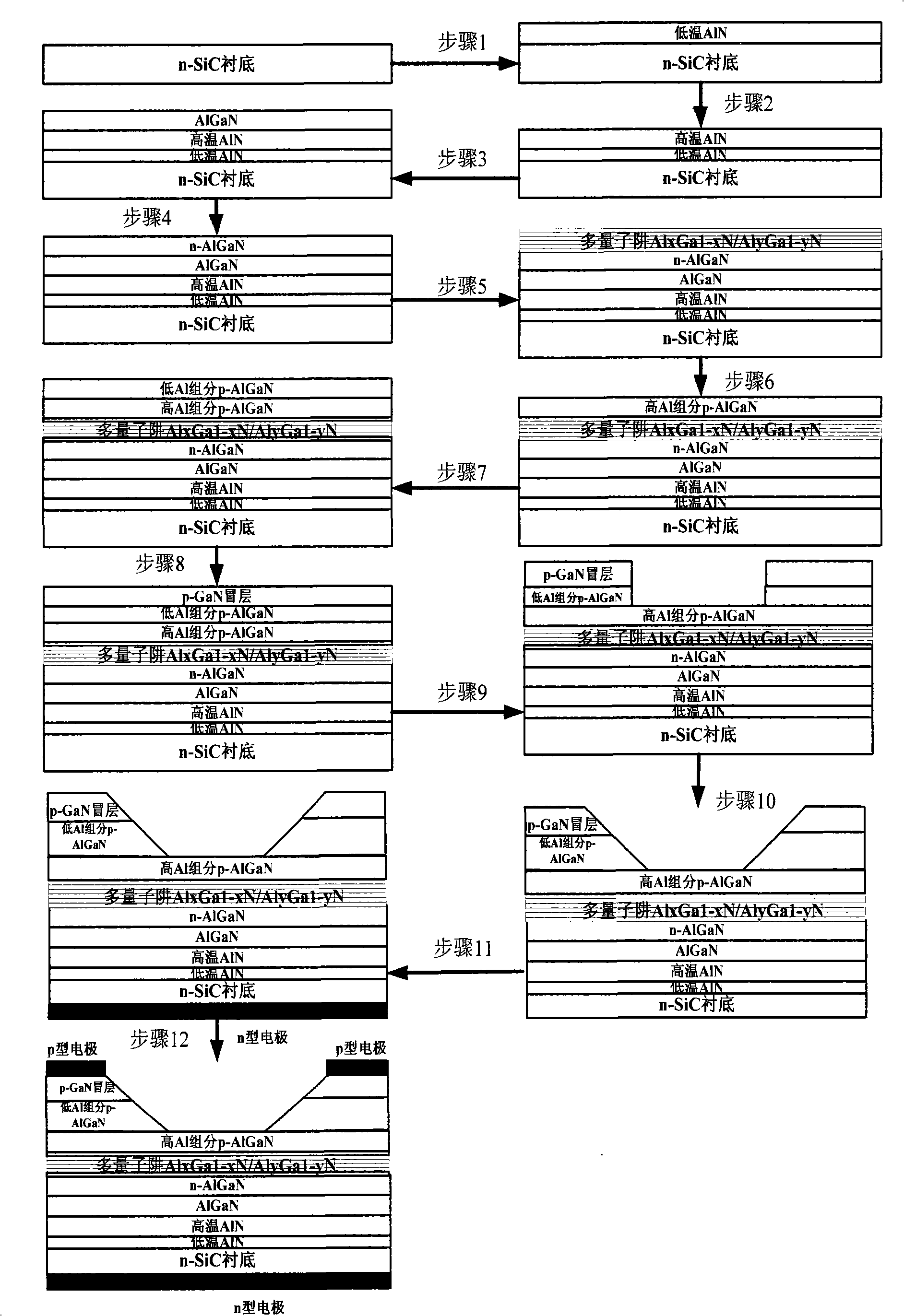
[0049] Embodiment 1. On the SiC substrate, a light exit window similar to a cone is fabricated by ICP dry and wet etching, and the steps are as follows:

[0050] Step 1: On the SiC substrate 1, a low-temperature AlN nucleation layer 2 is grown by MOCVD process.

[0051] The substrate temperature was lowered to 600°C, the growth pressure was maintained at 50Torr, the flow rate of hydrogen gas was 1500 sccm, the flow rate of ammonia gas was 1500 sccm, and the aluminum source with a flow rate of 28 μmol / min was introduced into the reaction chamber to grow a low-temperature AlN nucleation layer with a thickness of 10 nm.

[0052] Step 2, growing a high-temperature AlN nucleation layer 3 on the low-temperature AlN nucleation layer 2 .

[0053] Raise the growth temperature to 1050°C, keep the growth pressure at 50 Torr, the flow rate of hydrogen gas at 1500 sccm, the flow rate of ammonia gas at 1500 sccm, feed the aluminum source at a flow rate of 28 μmol / min into the reaction chamb...

Embodiment 2

[0080] Embodiment 2, on the SiC substrate, use ICP dry method and wet etching method to make a light exit window similar to a cone, the steps are as follows:

[0081] Step 1: On the SiC substrate 1, a low-temperature AlN nucleation layer 2 is grown by MOCVD process.

[0082] The substrate temperature was lowered to 600°C, the growth pressure was maintained at 50Torr, the flow rate of hydrogen gas was 1500 sccm, the flow rate of ammonia gas was 1500 sccm, and the aluminum source with a flow rate of 28 μmol / min was introduced into the reaction chamber to grow a low-temperature AlN nucleation layer with a thickness of 10 nm.

[0083] Step 2, growing a high-temperature AlN nucleation layer 3 on the low-temperature AlN nucleation layer 2 .

[0084] Raise the growth temperature to 1050°C, keep the growth pressure at 50 Torr, the flow rate of hydrogen gas at 1500 sccm, the flow rate of ammonia gas at 1500 sccm, feed the aluminum source at a flow rate of 28 μmol / min into the reaction ...

Embodiment 3

[0111] Embodiment 3, on the SiC substrate, a light exit window similar to a cone is fabricated by ICP dry and wet etching, and the steps are as follows:

[0112] Step 1: On the SiC substrate 1, a low-temperature AlN nucleation layer 2 is grown by MOCVD process.

[0113] The substrate temperature was lowered to 600°C, the growth pressure was maintained at 50Torr, the flow rate of hydrogen gas was 1500 sccm, the flow rate of ammonia gas was 1500 sccm, and the aluminum source with a flow rate of 28 μmol / min was introduced into the reaction chamber to grow a low-temperature AlN nucleation layer with a thickness of 10 nm.

[0114] Step 2, growing a high-temperature AlN nucleation layer 3 on the low-temperature AlN nucleation layer 2 .

[0115] Raise the growth temperature to 1050°C, keep the growth pressure at 50 Torr, the flow rate of hydrogen gas at 1500 sccm, the flow rate of ammonia gas at 1500 sccm, feed the aluminum source at a flow rate of 28 μmol / min into the reaction chamb...


PUM


Abstract

The invention discloses an AlGaN-based multiple quantum well uv-LED device based on a SiC substrate and a manufacturing method, relating to the technical field of micro-electronics. The device comprises a low-temperature AlN nucleating layer (2), a high-temperature AlN nucleating layer (3), an intrinsic AlGaN epitaxial layer (4), an n-AlGaN barrier layer (5), an active area (6), a p-AlGaN barrier layer (7), a low Al component p-shaped AlGaN layer (8), a p-shaped GaN capping layer (9) and a window area (10) arranged on the p-shaped GaN capping layer from bottom to top in sequence. The device etches the p-GaN capping layer to an electronic p-AlGaN barrier layer by a dry method to form a cylindrical emergent light window which is changed into a conical window by a secondary wet etching, so that the emergent aperture of the window is enlarged and the spread distance of the emergent light is simultaneously shortened. Due to adopting the method of etching, the device coarsens the surface of the electronic p-AlGaN barrier layer, thus further improving the emitting efficiency of the emergent light. In addition, the device has simple process, low cost, good repeatability and high reliability and can be used for water quality detection, medical probing, biopharming and white light illumination.

Description

technical field [0001] The invention belongs to the technical field of microelectronics and relates to a semiconductor device, in particular to a method for realizing a novel AlGaN-based multi-quantum well uv-LED device, which can be used in the fields of water treatment, medical treatment, biomedicine and white light illumination. Background technique [0002] As an outstanding representative of the third-generation semiconductor materials, III-V compound semiconductor materials have many excellent characteristics, especially in optical applications. The alloy {Ga(Al,In)N} composed of Ga, Al, In, N Can cover the entire visible light region and near ultraviolet light region. Moreover, the group III nitrides with wurtzite structure have direct band gaps, which are very suitable for the application of optoelectronic devices. Especially in the ultraviolet region, the AlGaN-based multi-quantum well uv-LED has shown great advantages, and has become one of the hot spots in the de...

Claims


Application Information

Patent Timeline
Patent Type & Authority Applications(China)
IPC IPC(8): H01L33/00
Inventor 郝跃杨凌马晓华周小伟李培咸
Owner XIDIAN UNIV
Why Eureka
Try Eureka