AlGaN-based uv-LED device on SiC substrate and manufacturing method

A technology of LED devices and substrates, applied in semiconductor devices, electrical components, circuits, etc., can solve the problems of long exit path, large mid-way light loss, and more ultraviolet light absorption, and achieve improved exit aperture, output power, and process simple effect

Inactive Publication Date: 2009-08-26
XIDIAN UNIV
View PDF0 Cites 7 Cited by
  • Summary
  • Abstract
  • Description
  • Claims
  • Application Information

AI Technical Summary

Problems solved by technology

In 2004, a 250nm LED was produced. The maximum power of a 200μ×200μ chip is close to 0.6mW, but the external quantum efficiency is only 0.01%.
As the emission wavelength decreases, the bottom buffer layer absorbs more and more ultraviolet light, which seriously affects the output light power and external quantum efficiency.
At present, the quality of the epitaxial layer is mainly improved by improving the structure of the device. However, the existing technology of em

Method used


Image

  • AlGaN-based uv-LED device on SiC substrate and manufacturing method
  • AlGaN-based uv-LED device on SiC substrate and manufacturing method
  • AlGaN-based uv-LED device on SiC substrate and manufacturing method

Examples


Embodiment 1

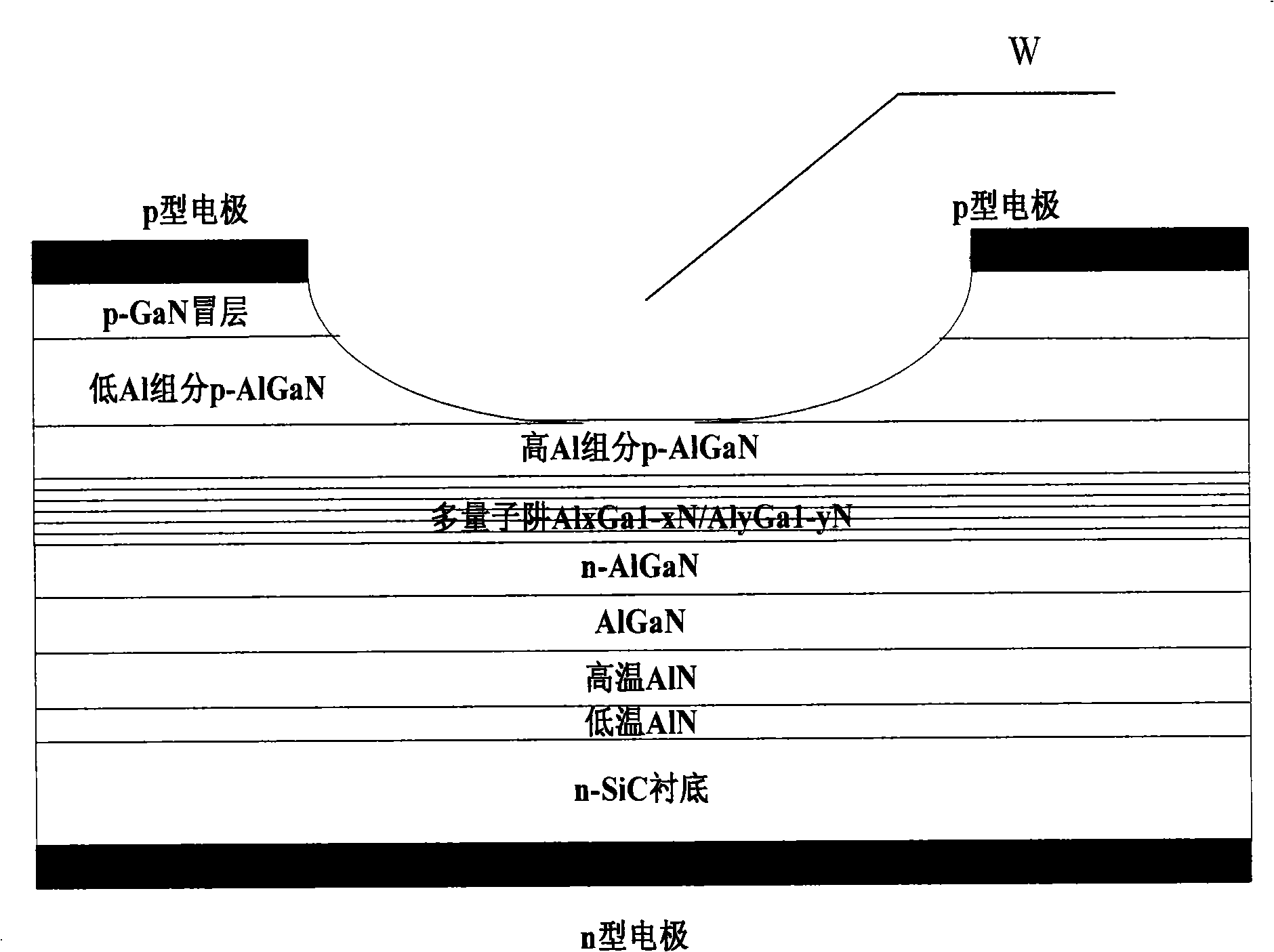
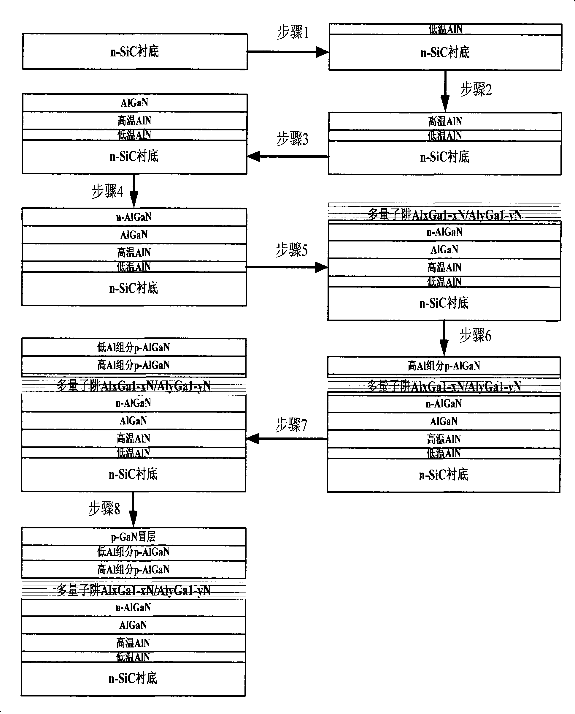
[0043] Embodiment 1, the fabrication of the device of the present invention includes three parts: material growth, window area fabrication and electrode fabrication.

[0044] 1. Reference figure 2 , the material growth steps are as follows:

[0045] In step 1, a low-temperature AlN nucleation layer is grown on the SiC substrate by MOCVD process.

[0046] The substrate temperature was lowered to 600°C, the growth pressure was maintained at 50Torr, the flow rate of hydrogen gas was 1500 sccm, the flow rate of ammonia gas was 1500 sccm, and the aluminum source with a flow rate of 23 μmol / min was introduced into the reaction chamber to grow a low-temperature AlN nucleation layer with a thickness of 7 nm.

[0047] Step 2, growing a high temperature AlN nucleation layer on the low temperature AlN nucleation layer.

[0048] Raise the growth temperature to 1050°C, keep the growth pressure at 50 Torr, the flow rate of hydrogen gas at 1500 sccm, the flow rate of ammonia gas at 1500 s...

Embodiment 2

[0079] Embodiment 2, the fabrication of the device of the present invention includes three parts: material growth, window area fabrication and electrode fabrication.

[0080] 1. Material growth steps:

[0081] The material growth steps are the same as in the first embodiment.

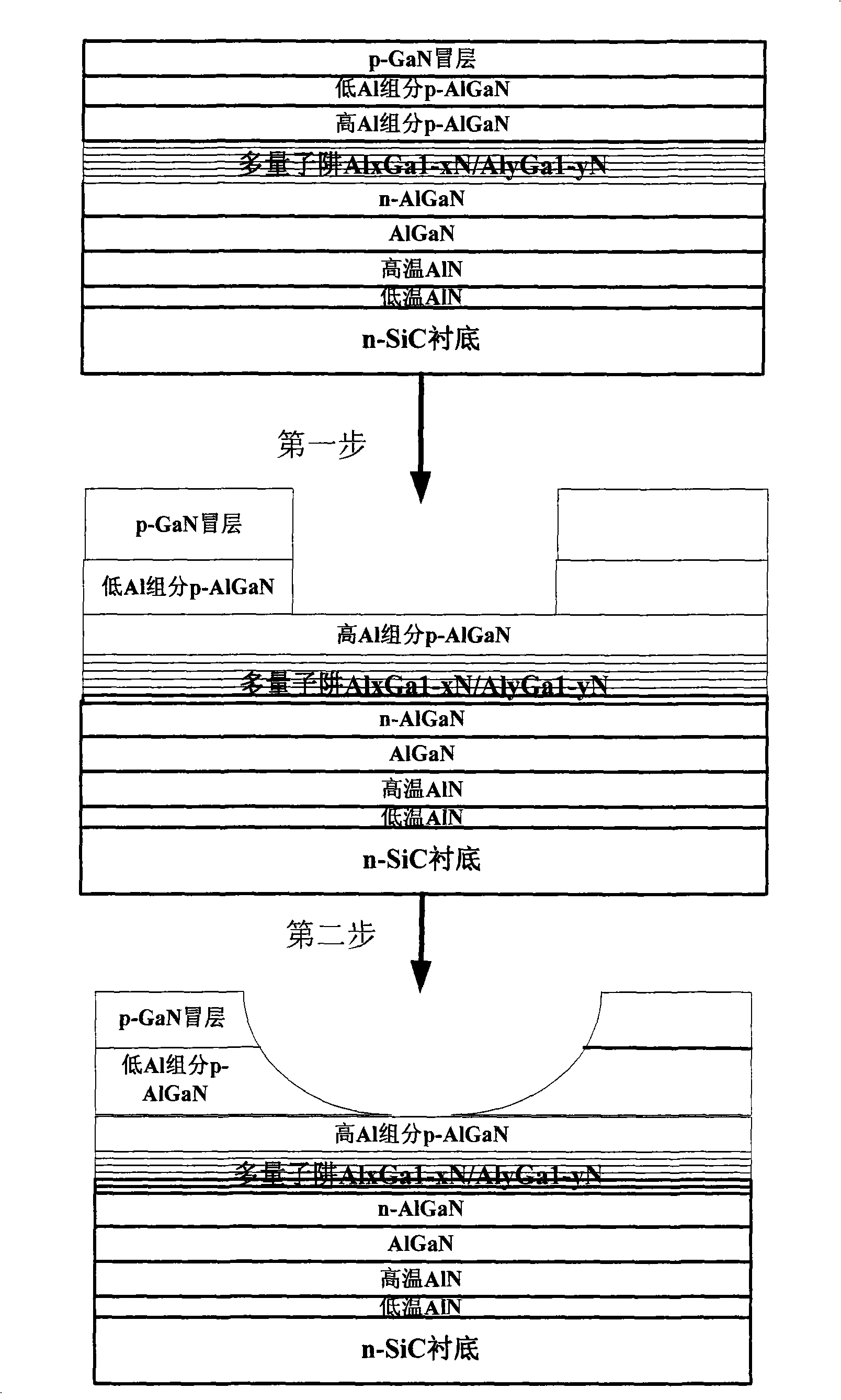
[0082] 2. The device window area is made as image 3 As shown, the specific steps are as follows:

[0083] The first step is to photoetch a circular window on the p-type GaN capping layer, and use ICP to etch the window area to the half of the p-type AlGaN barrier layer with low Al composition to form a cylindrical light exit window.

[0084] Shake the positive glue on the sample, the rotation speed is 5000 rpm, and then bake in an oven at 90°C for 15 minutes, and form the light exit window required for etching through photolithography and development;

[0085] Use ICP dry method to etch the p-type GaN layer to the p-type AlGaN layer with low Al composition, the etching depth is 90nm, and the gas use...

Embodiment 3

[0093] Embodiment 3, the fabrication of the device of the present invention includes three parts: material growth, window area fabrication and electrode fabrication.

[0094] 1. Material growth steps:

[0095] The material growth steps are the same as in the first embodiment.

[0096] 2. The device window area is made as image 3 As shown, the specific steps are as follows:

[0097] The first step is to photoetch a circular window on the p-type GaN capping layer, and use ICP to etch the window area to the half of the p-type low-Al component p-type AlGaN barrier layer to form a cylindrical light exit window.

[0098] Shake the positive glue on the sample, the rotation speed is 5000 rpm, and then bake in an oven at 90°C for 15 minutes, and form the light exit window required for etching through photolithography and development;

[0099] Use ICP dry method to etch the p-type GaN layer to the p-type AlGaN barrier layer with low Al composition, the etching depth is 90nm, and the...


PUM


Abstract

The invention discloses an AlGaN-based uv-LED device on a SiC substrate and a manufacturing method, relating to the technical field of micro-electronics and mainly solving the problem of low light-emitting efficiency. The device comprises a low-temperature AlN nucleating layer, a high-temperature AlN nucleating layer, an intrinsic AlGaN epitaxial layer, an n-AlGaN barrier layer, an active area, a p-AlGaN barrier layer, a low Al component p-shaped AlGaN layer, a p-shaped GaN capping layer and a window area arranged on the p-shaped GaN capping layer from bottom to top in sequence. The device etches the p-GaN capping layer to the low Al component p-AlGaN layer by a dry method to form a cylindrical emergent light window, and then the cylindrical emergent light window is etched by a photo-assisted wet method to be changed into a hemispheric-like window, so that the emergent aperture of the window is enlarged, the power and efficiency of the emergent light are improved and the window is especially suitable for manufacturing large-power uv-LED. The device has simple process, good repeatability and high reliability and can be used for water processing, medical treatment, biomedicine occasion and white light illumination.

Description

technical field [0001] The invention belongs to the technical field of microelectronics and relates to a semiconductor device, in particular to a method for realizing a novel AlGaN-based multi-quantum well uv-LED device, which can be used in the fields of water treatment, medical treatment, biomedicine and white light illumination. Background technique [0002] As an outstanding representative of the third-generation semiconductor materials, III-V compound semiconductor materials have many excellent characteristics, especially in optical applications. The alloy {Ga(Al,In)N} composed of Ga, Al, In, N Can cover the entire visible light region and near ultraviolet light region. Moreover, the group III nitrides with wurtzite structure have direct band gaps, which are very suitable for the application of optoelectronic devices. Especially in the ultraviolet region, the AlGaN-based multi-quantum well uv-LED has shown great advantages, and has become one of the hot spots in the de...

Claims


Application Information

Patent Timeline
IPC IPC(8): H01L33/00
Inventor 郝跃杨凌马晓华周小伟李培咸
Owner XIDIAN UNIV
Why Eureka
Try Eureka