

Ultraviolet LED element and fabricated method of AlGaN base sapphire substrate
A sapphire substrate and LED device technology, applied in semiconductor devices, electrical components, circuits, etc., can solve the problems of high light loss, long exit path, and more ultraviolet light absorption in the middle, so as to increase output power, increase exit aperture, The effect of simple process
- Summary
- Abstract
- Description
- Claims
- Application Information
AI Technical Summary
Problems solved by technology
Method used
Image

Examples
Embodiment 1
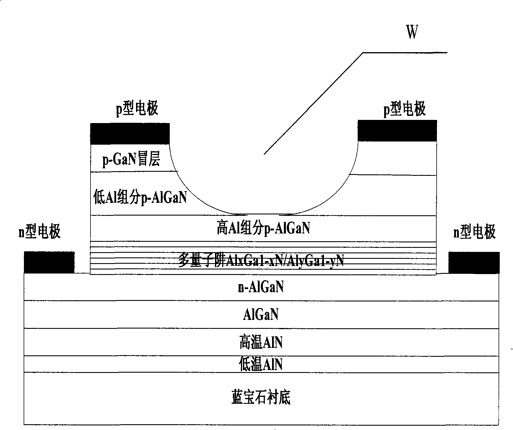
[0045] Embodiment 1, the fabrication of the device of the present invention includes three parts: material growth, window area fabrication and electrode fabrication.
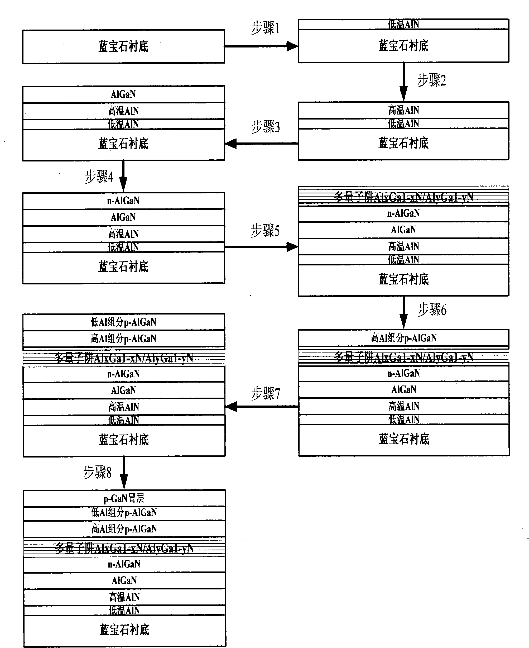
[0046] 1. Reference figure 2 , the material growth steps are as follows:
[0047] In step 1, a low-temperature AlN nucleation layer is grown on a sapphire substrate by MOCVD process.
[0048] The substrate temperature was lowered to 600°C, the growth pressure was maintained at 50Torr, the flow rate of hydrogen gas was 1500 sccm, the flow rate of ammonia gas was 1500 sccm, and the aluminum source with a flow rate of 23 μmol / min was introduced into the reaction chamber to grow a low-temperature AlN nucleation layer with a thickness of 7 nm.
[0049] Step 2, growing a high temperature AlN nucleation layer on the low temperature AlN nucleation layer.
[0050] Raise the growth temperature to 1050°C, keep the growth pressure at 50 Torr, the flow rate of hydrogen gas at 1500 sccm, the flow rate of ammonia gas at 150...
Embodiment 2
[0083] Embodiment 2, the fabrication of the device of the present invention includes three parts: material growth, window area fabrication and electrode fabrication.
[0084] 1. Material growth steps:
[0085] The material growth steps are the same as in the first embodiment.
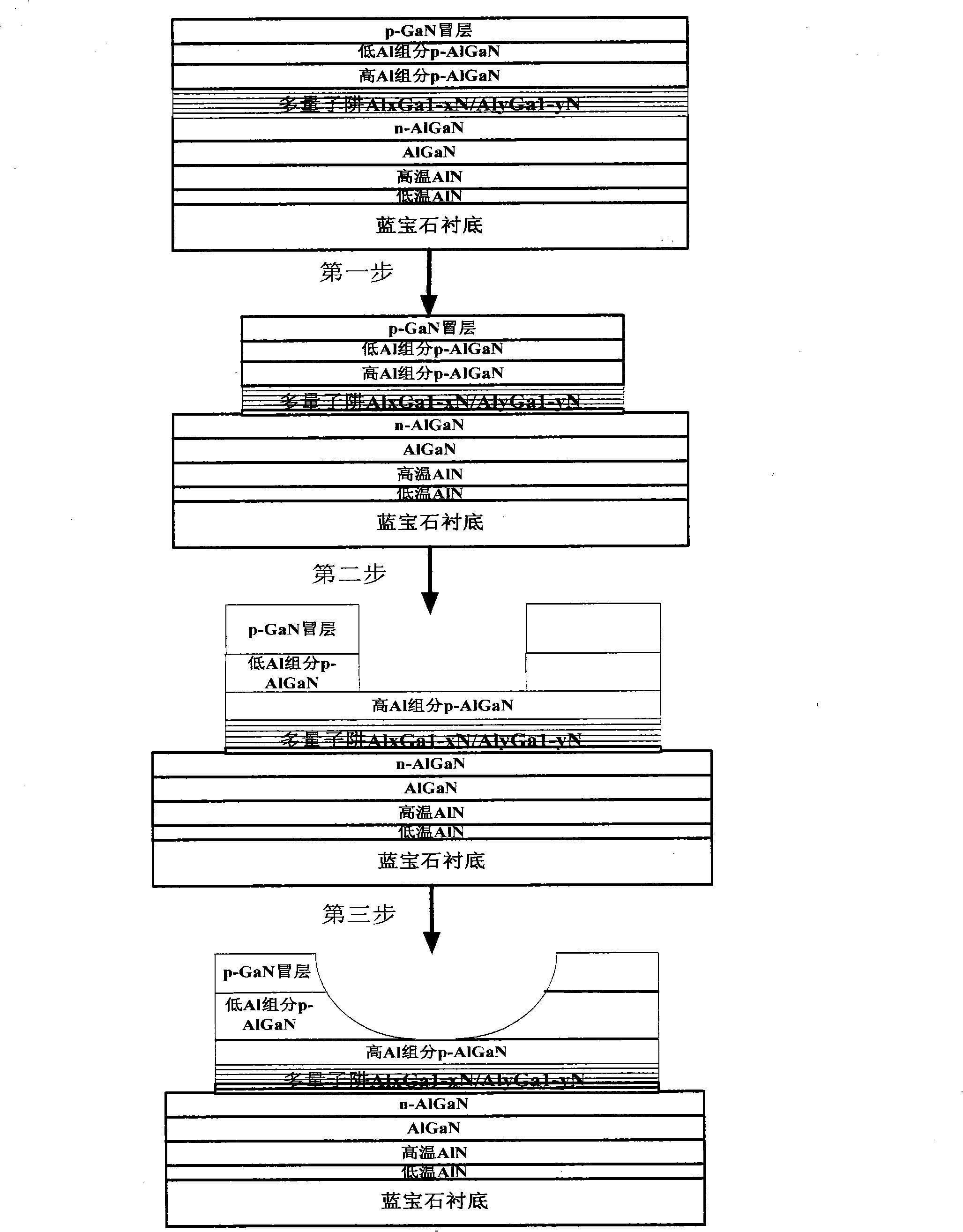
[0086] 2. The device window area is made as image 3 As shown, the specific steps are as follows:
[0087] The first step is to etch the mesa to the n-type AlGaN layer on the p-type GaN capping layer by using ICP or RIE process.
[0088] Deposit SiO with a thickness of about 300nm using electron beam evaporation equipment 2 layer as an etch mask layer. Due to the slow etch rate of AlGaN material, this step is added to form SiO on the sample 2 The double-layer mask pattern that works together with the photoresist is more conducive to protecting the surface of the unetched area;
[0089] Shake the positive glue on the sample sheet at a speed of 5000 rpm, and then bake it in an oven at a temperature ...
Embodiment 3
[0099] Embodiment 3, the fabrication of the device of the present invention includes three parts: material growth, window area fabrication and electrode fabrication.
[0100] 1. Material growth steps:
[0101] The material growth steps are the same as in the first embodiment.
[0102] 2. The device window area is made as image 3 As shown, the specific steps are as follows:
[0103] The first step is to etch the mesa to the n-type AlGaN layer on the p-type GaN capping layer by using ICP or RIE process.
[0104] Deposit SiO with a thickness of about 300nm using electron beam evaporation equipment 2 layer as an etch mask layer. Due to the slow etch rate of AlGaN material, this step is added to form SiO on the sample 2 The double-layer mask pattern that works together with the photoresist is more conducive to protecting the surface of the unetched area;
[0105] Shake the positive glue on the sample sheet at a speed of 5000 rpm, and then bake it in an oven at a temperature ...
PUM
 Abstract
Description
Claims
Application Information