Method for testing mechanical property and reliability of thin film material of micro-electromechanical system (MEMS) and device thereof

A technology of micro-electromechanical systems and thin-film materials, applied in the field of micro-electromechanical systems, can solve problems such as the damage and influence of the measured thin film cannot be eliminated, the sample clamping and alignment difficulties, and the preparation process are complicated, so as to achieve high test efficiency and simple test. , the effect of simple sample preparation

Inactive Publication Date: 2009-09-02
INST OF SEMICONDUCTORS - CHINESE ACAD OF SCI
View PDF0 Cites 51 Cited by
  • Summary
  • Abstract
  • Description
  • Claims
  • Application Information

AI Technical Summary

Problems solved by technology

[0005] However, the sample preparation process of these test methods is mostly complicated, and requires patterning processes such as etching on the film to be tested, and the damage and influence of the processing technology on the film to be teste

Method used


Image

  • Method for testing mechanical property and reliability of thin film material of micro-electromechanical system (MEMS) and device thereof
  • Method for testing mechanical property and reliability of thin film material of micro-electromechanical system (MEMS) and device thereof
  • Method for testing mechanical property and reliability of thin film material of micro-electromechanical system (MEMS) and device thereof

Examples


preparation example Construction

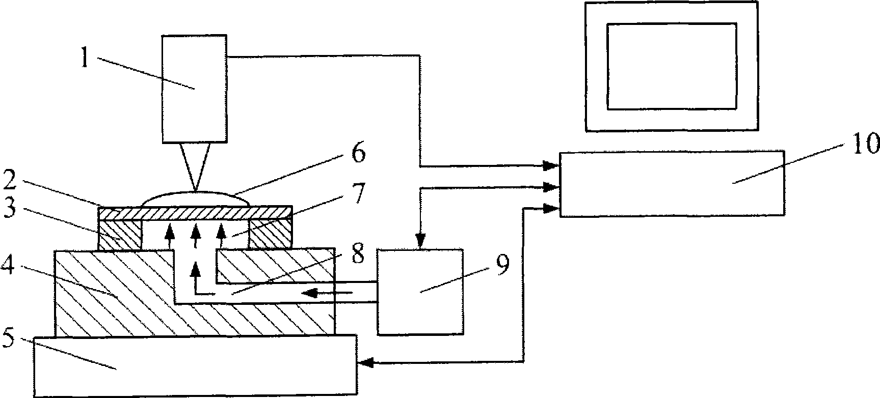
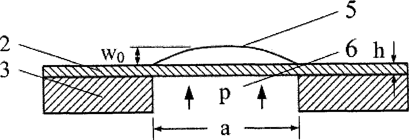
[0059] The preparation steps of the above-mentioned test structure are as follows: the measured material thin film 2 is deposited on the substrate 3, and the deposition process of the measured material thin film 2 can be traditional chemical vapor deposition (CVD), physical vapor deposition (PVD) Wait. Then, a thin film is deposited on the back of the substrate 3, and the thin film is used as a mask when etching the substrate 3, and the thin film is subjected to photolithography and dry etching to form pattern windows. The substrate 3 with the mask pattern on the back is placed in the wet etchant, and the substrate 3 exposed in the pattern window of the mask layer film is etched away to form a cavity 7, so that the measured material film 2 is partially The area forms a suspended membrane 6 .

[0060] The shape of the suspended membrane 6 is one of rectangle, square or circle, and an array with multiple suspended membranes 6 can be prepared on the same substrate 3 at the same ...


PUM


Abstract

The invention discloses a method for testing mechanical property and reliability of a thin film material of a micro-electromechanical system (MEMS) and a testing device thereof. A thin film testing structure with a suspended membrane is fixed on a sample platform with a gas passage and a differential pressure is imposed on one side of the suspended membrane to cause the other side of the suspended membrane to be deformed and heave; the deflection at the center of the membrane under the impressed pressure is measured, namely the maximum deflection of the membrane and the pressure is gradually increased to cause the suspended membrane to fracture; such parameters related to the mechanical property and reliability of the tested thin film material as plane strain modulus, Young modulus, Poisson ratio, residual stress, rupture strength and the like are extracted and obtained with the measurement of a pressure-deflection change curve and in accordance with a theory calculating model. The invention adopts a non-contact optical method, utilizes a data acquisition and control unit to automatically implement the measurement of the deflection and is characterized by simple sample preparation and testing, high measurement accuracy, convenient and flexible operation and high testing efficiency.

Description

technical field [0001] The invention relates to a micro-electro-mechanical system, in particular to a testing method and device for measuring the mechanical properties and reliability parameters of a micro-electro-mechanical system thin film material. Background technique [0002] Micro Electromechanical System (MEMS) refers to a micro electromechanical system that integrates micro sensors, actuators, signal processing and control circuits, interface circuits and power supplies. MEMS has the advantages of miniaturization, intelligence, multi-function, high integration and suitable for mass production, so it has broad application prospects in the fields of automobile, communication, biomedicine, consumer products, aerospace and national defense. With the continuous development and maturity of MEMS design methods and processing techniques, more and more MEMS devices have been successfully prepared, such as pressure sensors and resonators. [0003] The performance of MEMS devi...

Claims


Application Information

Patent Timeline
IPC IPC(8): G01N3/00
Inventor 杨晋玲周威杨富华
Owner INST OF SEMICONDUCTORS - CHINESE ACAD OF SCI
Why Eureka
Try Eureka