
Semiconductor device and manufacturing method thereof

A manufacturing method, semiconductor technology, applied in semiconductor/solid-state device manufacturing, semiconductor devices, electric solid-state devices, etc.

Inactive Publication Date: 2009-09-16
PANASONIC CORP
View PDF1 Cites 8 Cited by
  • Summary
  • Abstract
  • Description
  • Claims
  • Application Information

AI Technical Summary

Problems solved by technology

Therefore, in the semiconductor device described in Patent Document 1, both the advantages in the characteristics of the HBT and the advantages in the characteristics of the HFET cannot be achieved.

Method used


Image

  • Semiconductor device and manufacturing method thereof
  • Semiconductor device and manufacturing method thereof
  • Semiconductor device and manufacturing method thereof

Examples


Embodiment Construction

[0053] Hereinafter, an integrated circuit (Bi-HFET) of an HBT and an HFET in an embodiment of the present invention and a method of manufacturing the same will be described with reference to the drawings.

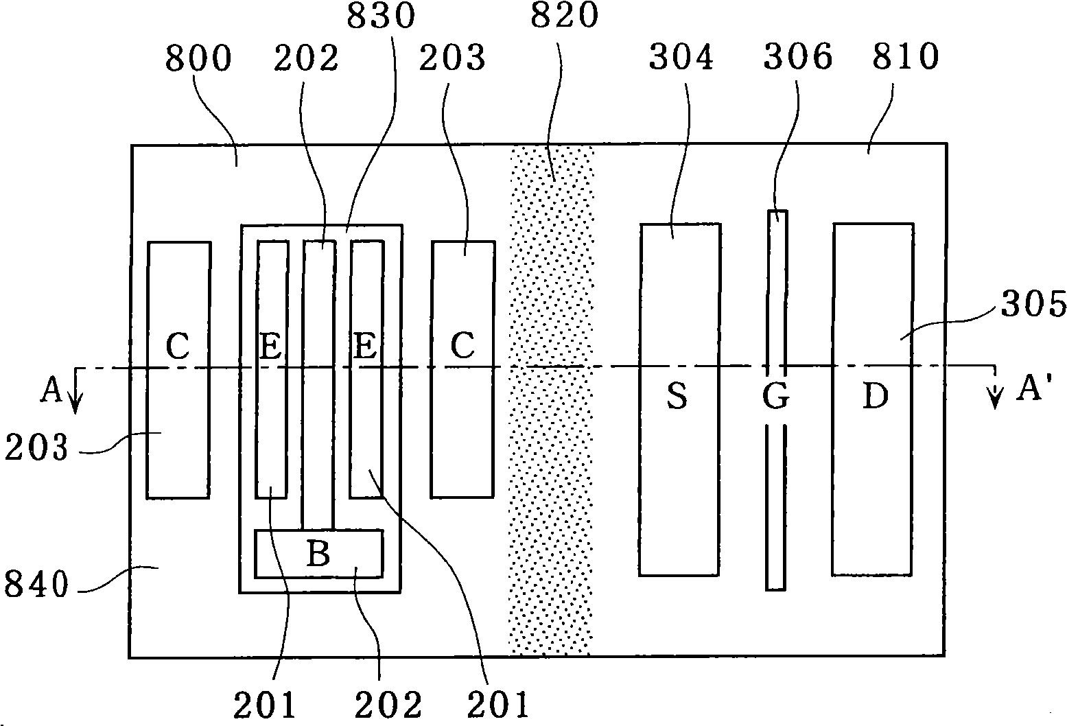
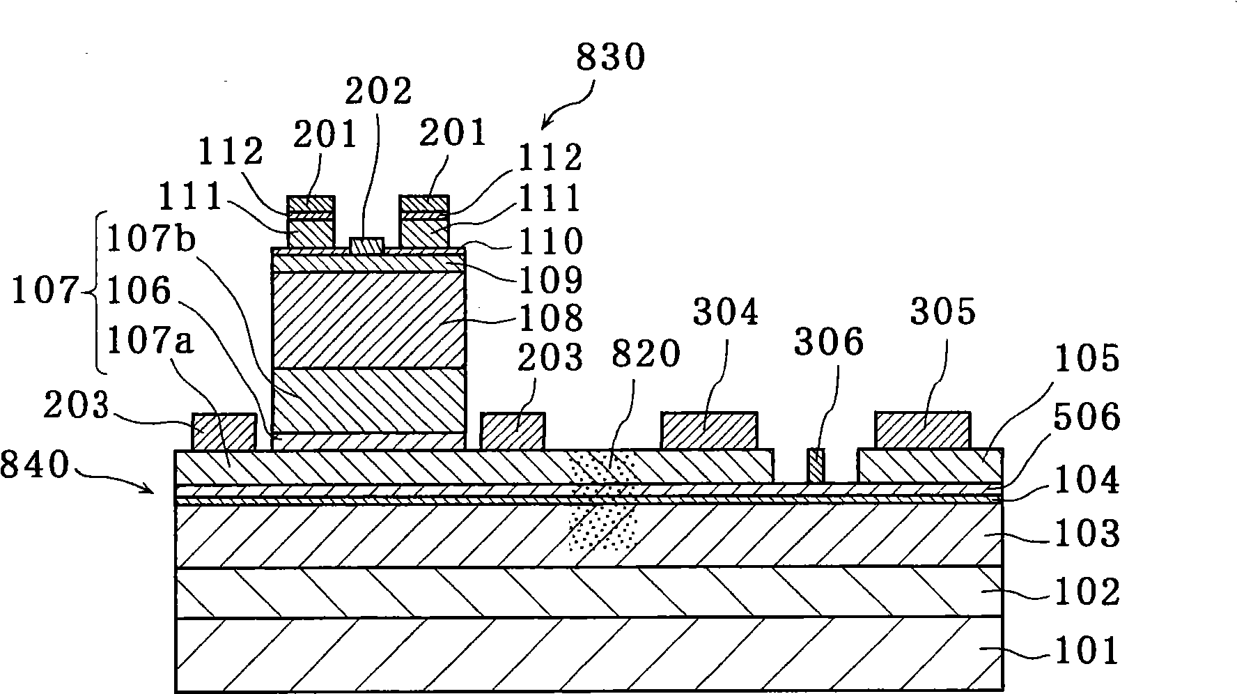
[0054] Figure 1A It is a plan view of the Bi-HFET according to this example. and, Figure 1B is a cross-sectional view of the structure of the Bi-HFET ( Figure 1A sectional view on line A-A').

[0055] This Bi-HFET is a semiconductor device having HBT and HFET formed on the same semiconductor substrate, and has a region 800 where the HBT is formed (HBT region) and a region 810 where the HFET is formed (HFET region). The HBT region 800 and the HFET region 810 are electrically isolated by an implant isolation region 820 .

[0056] In the HFET region 810 , a GaAs / AlGaAs superlattice layer 102 , an AlGaAs barrier layer 103 , an InGaAs channel layer 104 , an electron supply layer 506 and a GaAs cladding layer 105 are sequentially stacked on a semi-insulating GaAs substrate...


PUM


Abstract

The present invention has as an objective to provide: a semiconductor device to satisfy both of the trade-off characteristic advantages of the HBT; and the HFET and a manufacturing method thereof. The semiconductor device in the present invention is an HBT and HFET integrated circuit. The HBT includes a sub-collector layer, a GaAs collector layer, a GaAs base layer, and an InGaP emitter layer which are sequentially stacked. The sub-collector layer includes a GaAs external sub-collector region, and a GaAs internal sub-collector region disposed on the GaAs external sub-collector region. A mesa-shaped collector part and a collector electrode are separately formed on the GaAs external sub-collector region. The HFET includes a GaAs cap layer, a source electrode, and a drain electrode, the GaAs cap layer including portion of the GaAs external sub-collector region, and the source electrode and the drain electrode being formed on the GaAs cap layer.

Description

technical field [0001] The present invention relates to an integrated circuit (Bi-HFET) of HBT and HFET used as a high-frequency semiconductor device and its manufacturing method. Background technique [0002] A heterojunction bipolar transistor (HBT) in which a semiconductor with a large bandgap is used for the emitter is being put into practical use as a high-frequency analog element used in mobile phones and the like. In particular, InGaP / GaAsHBTs using InGaP (indium gallium phosphide) in the emitter are expected to be widely used in the future as devices with low temperature dependence and high reliability. [0003] Recently, research and development of an integrated circuit in which HBTs and HFETs are mixed is underway, such as controlling a power amplifier (PA) made of HBTs through a switching element (SW) made of heterojunction field effect transistors (HFETs). Therefore, a Bi-HFET processing technology that forms HBT and HFET on the same substrate has attracted atte...

Claims


Application Information

Patent Timeline
Patent Type & Authority Applications(China)
IPC IPC(8): H01L27/06H01L29/417H01L29/737H01L29/778H01L21/8248H01L21/28
CPCH01L27/0605H01L29/802H01L27/0623H01L29/7371H01L21/8248
Inventor 村山启一田村彰良宫本裕孝宫岛贤一
Owner PANASONIC CORP
Learn More