SOILDMOS transistor with changeover body connection

A transistor and body region technology, applied in semiconductor devices, electrical components, circuits, etc., can solve the problem that the local SOI structure cannot fully improve the performance of the device, and cannot reduce the heat dissipation capacity of the drain-source capacitor, so as to suppress the floating body. effect, reduce the self-heating effect, and improve the effect of heat dissipation

Inactive Publication Date: 2009-09-16
HARBIN ENG UNIV
View PDF1 Cites 9 Cited by
  • Summary
  • Abstract
  • Description
  • Claims
  • Application Information

AI Technical Summary

Problems solved by technology

However, these structures cannot make the device meet the requirements of reducing the drain-source capacitance and improving the heat dis

Method used


Image

  • SOILDMOS transistor with changeover body connection
  • SOILDMOS transistor with changeover body connection
  • SOILDMOS transistor with changeover body connection

Examples


Embodiment Construction

[0018] The present invention will be described in more detail below in conjunction with the accompanying drawings:

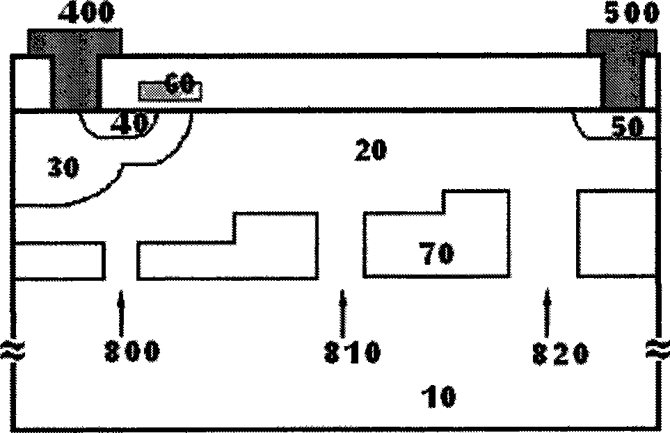
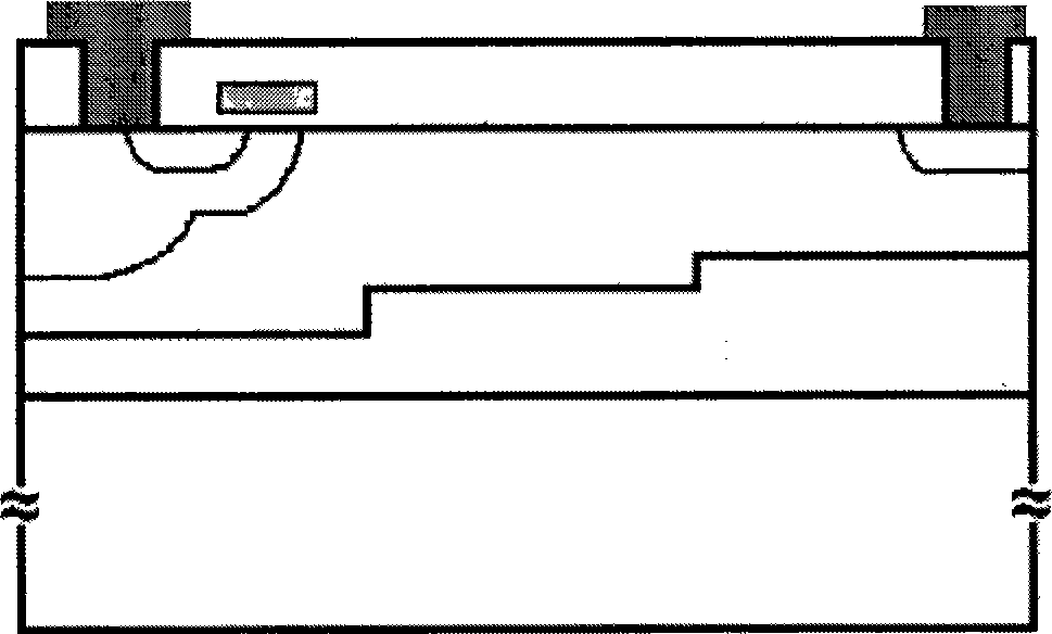
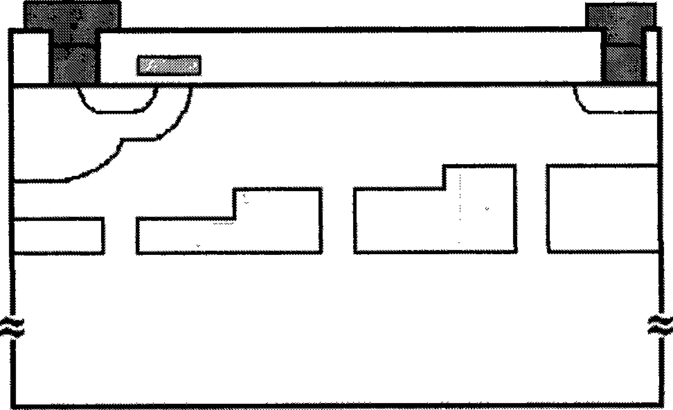
[0019] combine figure 1 , the SOILDMOS transistor of the present invention includes N + Source region 40, P body region 30, N - Drift zone 20, N + The drain region 50 , the aluminum metal source electrode 400 , the aluminum metal drain electrode 500 , and the polysilicon gate electrode 60 . Buried SiO 2 The layer 70 has windows 800, 810, 820 with graded widths so that the SOI layer (active region) is connected to the silicon substrate 1. According to the electric field distribution and temperature distribution during operation of the device, the window width relationship is determined as W 800 810 820 . figure 2 It is a schematic diagram of the cross-sectional structure of a stepped buried oxygen SOILDMOS transistor. image 3 It is a schematic diagram of the cross-sectional structure of a uniform body-connected SOI LDMOS transistor. figure 1 same. Figu...


PUM


Abstract

The invention provides an SOILDMOS transistor with changeover body connection, comprising a source region (40), a body region (30), a drift region (20), a drain region (50), a source electrode (400), a drain electrode (500) and a gate electrode (60). The invention is characterized in that an embedded dielectric layer (70) is provided with windows (800, 810 and 820) which have gradually changed widths and connect an SOI layer and a substrate semiconductor. In the SOILDMOS transistor with changeover body connection, the SOI layer (active region) and the substrate semiconductor can be connected by optimally designing the width of the windows with gradually changed widths of the embedded dielectric layer. Cavities generated by collision ionization can flow out from the substrate. Meanwhile, joule heat generated in a device region can effectively flow toward heat sink of the substrate, which not only can reduce self-heating effect but also can depress floating body effect.

Description

(1) Technical field [0001] The present invention relates to a transistor, in particular to a silicon-on-insulator (SOI) laterally diffused metal oxide semiconductor field effect transistor (LDMOSFET), in particular to a SOILDMOS transistor with a gradient body connection. (2) Background technology [0002] SOI high-voltage integrated circuits based on SOI lateral high-voltage devices, as an emerging branch in the field of intelligent power integrated circuits, have developed rapidly in recent years. It integrates SOI technology, microelectronic technology and power electronic technology, and provides a new type of switching circuit with high speed, high integration, low power consumption and radiation resistance for various power conversion and energy processing devices. , aerospace, power electronics and other high-tech industries have a very wide range of application prospects. SOI LDMOS transistors have the characteristics of high speed, low power consumption, high integ...

Claims


Application Information

Patent Timeline
IPC IPC(8): H01L29/78H01L29/06
Inventor 王颖曹菲赵旦峰葛梅
Owner HARBIN ENG UNIV
Why Eureka
Try Eureka