Method for producing silicon carbide substrate and silicon carbide substrate
A silicon carbide substrate and silicon carbide technology, applied in chemical instruments and methods, semiconductor/solid-state device manufacturing, post-processing details, etc., can solve the problems of increased cost, low productivity, low polishing efficiency, etc., and achieve the goal of improving flatness Effect
- Summary
- Abstract
- Description
- Claims
- Application Information
AI Technical Summary
Problems solved by technology
Method used
Image


Examples
example 1
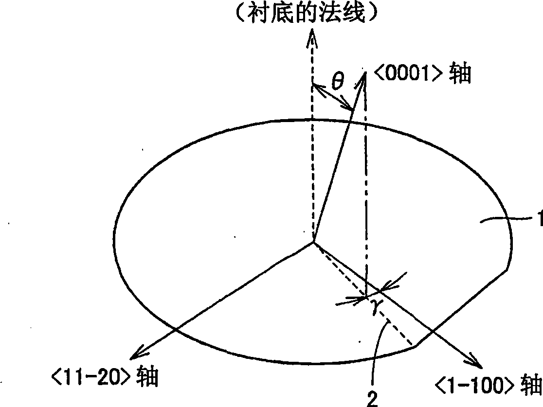
[0047] Such as Figure 6 As shown, a 2-inch substrate 51 of 6H-SiC, the (0001) surface of which was polished to a mirror surface, was set into a susceptor 52 of a hydrogen etching furnace. Regarding the surface orientation of the main surface in the SiC substrate, the inclination angle from the (0001) plane to the (1-100) plane was set to 0.03° to 0.5°. The susceptor 52 in the furnace is made of SiC-coated high-purity graphite, and the heat insulator 53 is made of fibrous graphite. A coil 54 is arranged on the periphery of the furnace through a quartz chamber 55, and a high-frequency current is fed to the coil for induction heating the SiC substrate in the furnace. The temperature at the underside of the susceptor was measured with a radiation thermometer, the induced current was controlled, and the temperature was set to 1450°C. at 0.1cm 3 6N high-purity hydrogen was fed into the furnace per min, and the furnace was evacuated and replaced with 3 kPa hydrogen for performing...
example 2
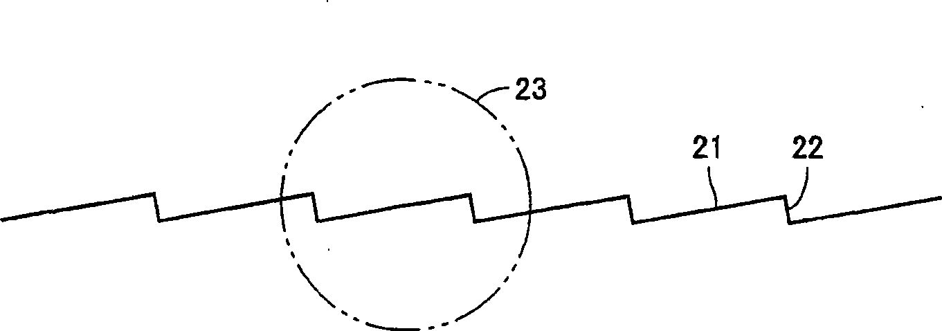
[0050] Similar to Example 1, a SiC substrate was produced with respect to a substrate having a main surface whose surface orientation was inclined by 0.02° from the (0001) plane to the (1-100) plane. As a result, it was observed by AFM as Figure 4 The bowl-shaped depression defect (spiral depression) shown. exist Figure 4 The minimum radius of curvature of the step presented on the deepest periphery of the central portion of the shown depression (critical radius; corresponding to Figure 4 1 / 4) of the distance between the two arrows shown is 725 nm. Steps from screw dislocations are hardly coupled with steps due to substrate inclination due to tilting from the (0001) plane of the substrate when, in the substrate, the initially existing step width is greater than the minimum radius of curvature of the helical depression , for bowl-shaped etching, a spiral depression is formed. On the other hand, when the step width is smaller than the minimum radius of curvature, no helic...
PUM
| Property | Measurement | Unit |
|---|---|---|
| Surface flatness | aaaaa | aaaaa |
Abstract
Description
Claims
Application Information
 - Generate Ideas
- Intellectual Property
- Life Sciences
- Materials
- Tech Scout
- Unparalleled Data Quality
- Higher Quality Content
- 60% Fewer Hallucinations
Browse by: Latest US Patents, China's latest patents, Technical Efficacy Thesaurus, Application Domain, Technology Topic, Popular Technical Reports.
© 2025 PatSnap. All rights reserved.Legal|Privacy policy|Modern Slavery Act Transparency Statement|Sitemap|About US| Contact US: help@patsnap.com