Nanometer silica film three-layer stacked solar cell and preparation method thereof

A technology of nano-silicon thin film and stacked solar, which is applied in coating, circuit, photovoltaic power generation, etc., can solve the problems of thin-film solar cell efficiency decline, large optical band gap of amorphous silicon, etc., and achieve low light-induced attenuation effect, band Gap adjustable range is high, the effect of no pollution to the environment

Inactive Publication Date: 2009-09-23
JIANGSU POLYTECHNIC UNIVERSITY +1
View PDF0 Cites 6 Cited by
  • Summary
  • Abstract
  • Description
  • Claims
  • Application Information

AI Technical Summary

Problems solved by technology

In the current silicon-based stacked thin film solar cells, nano-silicon thin films are usually used as the middle cell and the bottom cell, while the top cell is still made of amorphous silicon, mainly due to the large optical band gap of amorphous silicon, but such thin-film solar cells There is still a large efficiency decline problem

Method used


Image

  • Nanometer silica film three-layer stacked solar cell and preparation method thereof
  • Nanometer silica film three-layer stacked solar cell and preparation method thereof
  • Nanometer silica film three-layer stacked solar cell and preparation method thereof

Examples


Embodiment Construction

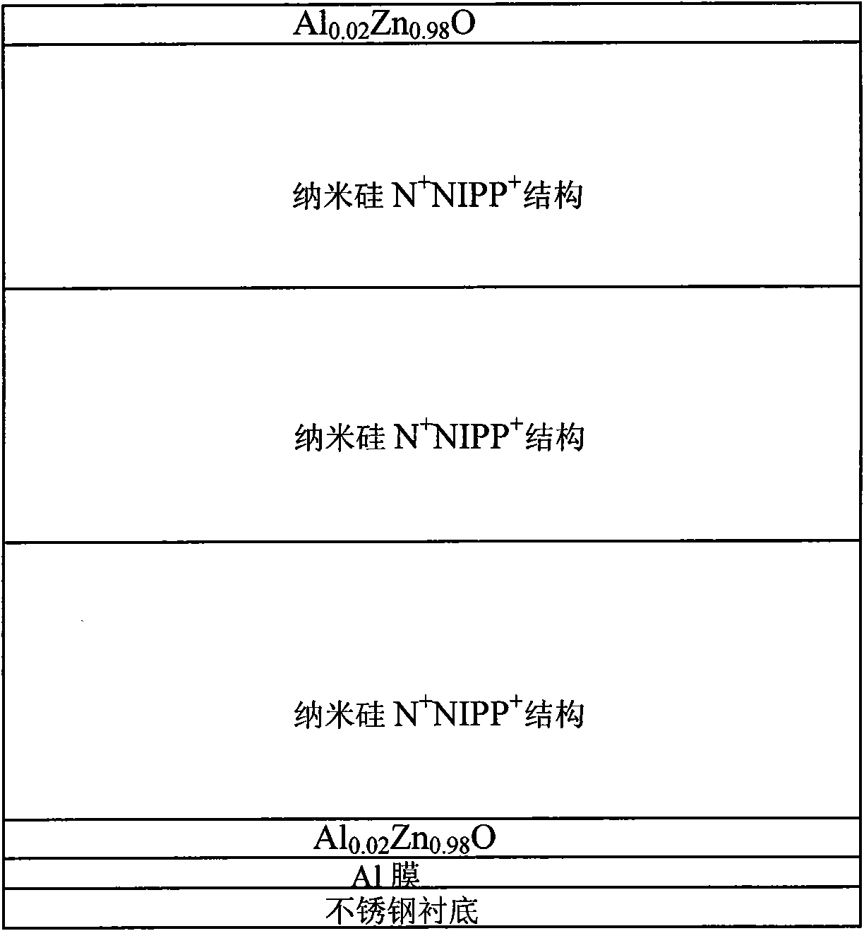
[0027] 1. Structural design of solar cells

[0028] Design top cell, middle cell and bottom cell as N on stainless steel substrate + NIPP + Structured nano-silicon thin-film triple-stack solar cells. increase N + Layer, P + It is to reduce contact resistance, increase short-circuit current and open-circuit voltage; at the same time, the existence of P layer and N layer makes I / P, N / P interface energy band mismatch transition slowly, reducing interface state density, thereby increasing open-circuit voltage and fill factor.

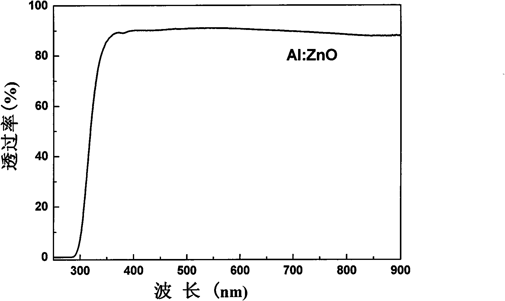
[0029] Using Al x Zn 1-x The O(x=0.02) / Al composite back electrode enhances the reflection of long-wavelength light, increases the light absorption and utilization of the solar cell, and prevents Al from diffusing into the cell. The textured structure of the upper electrode increases light absorption.

[0030] 2. Preparation of triple stack solar cells

[0031] 2.1 Cleaning of the substrate sheet

[0032] The stainless steel substrate was ultrasoni...


PUM

PropertyMeasurementUnit
particle sizeaaaaaaaaaa
crystallinityaaaaaaaaaa

Abstract

The invention relates to a film solar cell and a preparation method thereof, in particular to a nanometer silica film three-layer stacked solar cell and a preparation method thereof. The method of plasma enhanced chemical vapor deposition (PECVD) is adopted for preparing a hydrogenated nanometer silica film (nc-Si:H). An nc-Si:H/nc-Si:H/nc-Si:H film three-layer stacked solar cell is prepared on a soft metal or polyimide film substrate. The top cell, the middle cell and the bottom cell adopt the N<+>NIPP<+> structure. The method of radio frequency sputtering is adopted for depositing an Al/AlxZn1-xO double-layer back electrode and an AlxZn1-xO film upper electrode. The invention avoids the use of amorphous silicon and expensive amorphous germanium silicon; the relatively thinner nanometer silica film three-layer stacked solar cell with high efficiency and stability is obtained on the soft substrate by taking advantage of the adjustable scope of the band gap of nanometer silica width, the relatively higher absorption coefficient and lower photoinduced damping effect. The invention achieves simple process and low cost of the used materials and causes no pollution to the environment.

Description

technical field [0001] The invention relates to a thin-film solar cell and a preparation method thereof, in particular to a thin-film solar cell with a three-layer structure prepared by using nano-silicon thin film materials. Background technique [0002] With the increasingly serious energy crisis and environmental pollution, the development of renewable clean energy has become one of the major strategic issues in the international scope. Solar energy is an inexhaustible clean energy source, therefore, the development and utilization of solar energy has become a strategic decision for sustainable energy development in countries all over the world. Solar power generation is an important means to utilize solar energy economically on a large scale. Therefore, the research on large anode batteries has been paid more and more attention by countries all over the world. [0003] Amorphous silicon thin-film solar cell is a traditional silicon-based thin-film solar cell. Due to th...

Claims


Application Information

Patent Timeline
Patent Type & Authority Applications(China)
IPC IPC(8): H01L31/042H01L31/18C23C14/34C23C14/14C23C14/16C23C14/08C23C16/44C23C16/24
CPCY02E10/50Y02P70/50
Inventor 丁建宁袁宁一程广贵王秀琴何宇亮
Owner JIANGSU POLYTECHNIC UNIVERSITY
Why Eureka
Try Eureka