Amplifying element and manufacturing method thereof

一种放大元件、区域的技术,应用在放大器、半导体/固态器件制造、电气元件等方向,能够解决增益变小、电流降低等问题,达到低输出阻抗、高输入阻抗、静电击穿容量高的效果

Active Publication Date: 2009-09-30
SANYO ELECTRIC CO LTD +1
View PDF1 Cites 10 Cited by
  • Summary
  • Abstract
  • Description
  • Claims
  • Application Information

AI Technical Summary

Problems solved by technology

[0014] However, as mentioned above, in order to reduce the input capacitance Cin, the area of ​​the J-FET must be reduced, resulting in a reduction in the controllable current and a reduction in the gain
That is, the gain and the input capacitance Cin are in a trade-off relationship, and there is a limit to gain improvement for simple and inexpensive amplifier elements using J-FETs.

Method used


Image

  • Amplifying element and manufacturing method thereof
  • Amplifying element and manufacturing method thereof
  • Amplifying element and manufacturing method thereof

Examples


Embodiment Construction

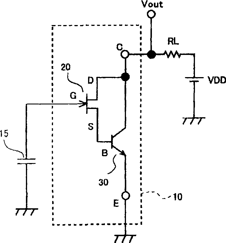
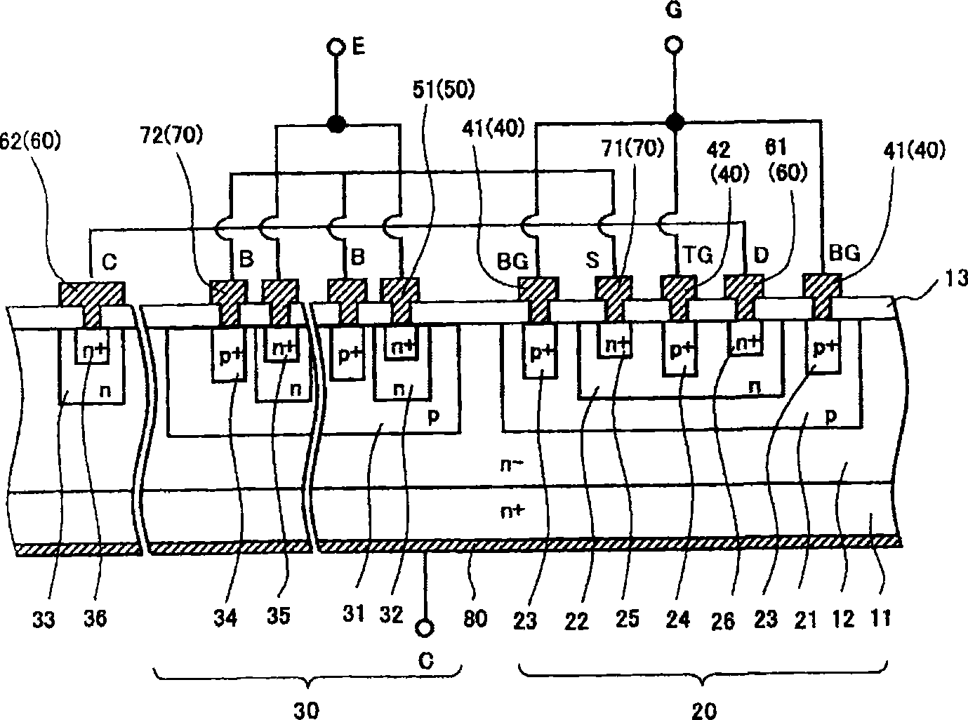
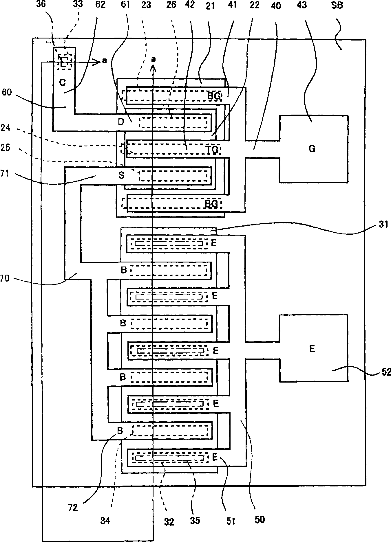
[0057] refer to Figure 1 to Figure 10 , taking the following case as an example to describe the embodiment of the present invention, that is, the case where an n-channel type J-FET and an npn bipolar transistor are integrated on an n-type semiconductor substrate.

[0058] figure 1 It is a circuit diagram showing a connection example of the amplifier element 10 of this embodiment.

[0059] Amplifying element 10 is the element that is connected with electret condenser microphone (ECM) 15 and carries out impedance conversion and amplification, and junction field effect transistor (J-FET) 20 and bipolar transistor 30 are integrated on a conductive type semiconductor substrate .

[0060] The ECM 15 arranges a vibrating membrane (vibrating plate) and electrodes facing it in a housing, and movement of the vibrating membrane due to sound is taken out as a change in capacitance between the vibrating membrane and the electrodes. The vibrating film is made of, for example, a polymer...


PUM


Abstract

The present invention provides an amplifying element and manufacturing method thereof. An amplifier integrated circuit element or J-FET is used for impedance conversion and amplification of ECM. The amplifier integrated circuit element has advantages of allowing an appropriate gain to be set by adjusting a circuit constant, and of producing a higher gain than the J-FET; but also has a problem of having a complicated circuit configuration and requiring high costs. On the other hand, using only the J-FET has also problems of outputting a voltage insufficiently amplified and producing a low gain. The invention provides a discrete element in which: a J-FET and a bipolar transistor are integrated on one chip; a source region of the J-FET is connected to a base region of the bipolar transistor; and a drain region of the J-FET is connected to a collector region of the bipolar transistor. Accordingly, an ECM amplifying element with high input impedance and low output impedance can be achieved.

Description

technical field [0001] The present invention relates to an amplifying element and its manufacturing method, in particular to a preferred amplifying element for an amplifying device and its manufacturing method. Background technique [0002] In order to perform impedance conversion and amplification of an electret condenser microphone (Electret Condenser Microphone: hereinafter referred to as ECM), for example, a junction field effect transistor (Junction FieldEffect Transistor: hereinafter referred to as J-FET) or an amplifying integrated circuit element (such as Refer to Patent Document 1 and Patent Document 2). [0003] Figure 11 It is a circuit diagram showing a conventional ECM 115 and an amplifying element 110 connected thereto. One end of the ECM 115 is connected to the gate G of the J-FET 110 which is an amplification element, one end of the J-FET 110 is grounded, and the other end is connected to a load resistor RL. Since the output impedance of the ECM 115 is hig...

Claims


Application Information

Patent Timeline
Patent Type & Authority Applications(China)
IPC IPC(8): H03F3/187H03F1/30H01L27/06H01L21/8248
CPCH03F3/1855
Inventor 小野寺荣男
Owner SANYO ELECTRIC CO LTD
Why Eureka
Try Eureka