Organic solar cell adopting weak epitaxial growth film as donor

A weak epitaxial growth and solar cell technology, applied in the field of organic solar cells, can solve the problems of increasing the complexity and cost of device preparation, limiting device performance, short-circuiting of thin-film devices, etc., to achieve effective transmission, overcome roughness increase, and device The effect of performance improvement

Inactive Publication Date: 2009-10-21
CHANGCHUN INST OF APPLIED CHEMISTRY - CHINESE ACAD OF SCI
View PDF1 Cites 14 Cited by
  • Summary
  • Abstract
  • Description
  • Claims
  • Application Information

AI Technical Summary

Problems solved by technology

However, due to the need for carrier gas transportation and precise control of the carrier gas flow rate, the cost is high and the experimental repeatability is poor.
In addition, due to the low substrate temperature (generally below 50°C), the grain size of the thin film is small and the mobility is low, which limits the further improvement of device performance.
[0005] On the other hand, researchers tried to increase the substrate temperature during deposition of organic small molecule fi

Method used


Image

  • Organic solar cell adopting weak epitaxial growth film as donor
  • Organic solar cell adopting weak epitaxial growth film as donor
  • Organic solar cell adopting weak epitaxial growth film as donor

Examples


Embodiment 1

[0036] A kind of donor that the present invention adopts the preparation method of the organic solar cell of weak epitaxial growth thin film, its steps and conditions are as follows:

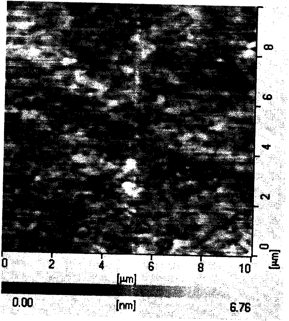
[0037] Spin-coat PEDOT / PSS conductive coating 2 on the surface of ITO glass 1, vacuum-deposit 10 nanometers of induction layer 3, 50 nanometers of donor material 4, 60 nanometers of acceptor material layer 6, and 5 nanometers on the PEDOT / PSS surface The metal electrode buffer layer 7 is finally deposited with a stencil with an area of ​​0.0314cm 2 , Ag with a thickness of 100 nm as the cathode 8 is formed as Image 6 Device configuration shown. The background vacuum is 8×10 -4 Pa, substrate temperature 155°C, deposition rate 1 nm / min, induction layer material is BP2T, donor material is ZnPc, acceptor material is C60, metal electrode buffer layer is Alq3.

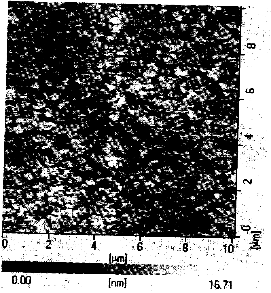
[0038] figure 1 It is the atomic force topography diagram of the surface of ITO conductive glass, and the surface roughness is 2.64nm. ...

Embodiment 2

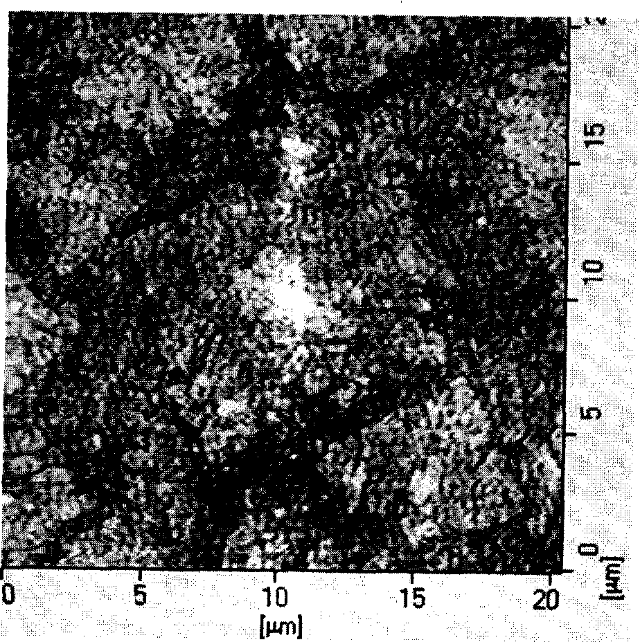
[0050] A layer of PEDOT / PSS 2 was spin-coated on the surface of ITO glass 1, and a 12-nanometer induction layer 3, a 10-nanometer donor material 4, and a blend layer of 15-nanometer donor material and acceptor material were vacuum-deposited sequentially on the surface of PEDOT:PSS 5. A receptor material layer 6 of 40 nanometers, a metal electrode buffer layer 7 of 0.5 nanometers, and finally deposit a layer with an area of ​​0.0314 cm by using a stencil 2 , Al with a thickness of 100 nm as the cathode 8 is formed as Figure 8 Device configuration shown. The background vacuum is 8×10 -4 Pa, the substrate temperature is 155°C, the deposition rate is 1 nm / min, the material of the induction layer is BP2T, the material of the donor is ZnPc, the material of the acceptor is C60, and the buffer layer of the metal electrode is LiF.

[0051] Figure 9 is adopted Figure 8 The second device configuration shown, the current-voltage curve of the solar cell with weak epitaxial growth fi...

Embodiment 3

[0057] On the surface of ITO glass 1, a 2-nanometer induction layer 3, a 60-nanometer blend layer 5 of a donor material and an acceptor material, and a 10-nanometer metal electrode buffer layer 7 are vacuum-deposited in sequence, and finally a layer with an area of ​​0.0314 cm is deposited using a stencil. 2 , Al with a thickness of 100 nm as the cathode 8 is formed as Figure 10 Device configuration shown. The background vacuum is 8×10 -4 Pa, substrate temperature 155°C, deposition rate 1 nm / min, induction layer material is BP2T, donor material is ZnPc, acceptor material is C60, metal electrode buffer layer is Alq3.

[0058] Figure 11 is adopted Figure 10 The third device configuration shown, the current-voltage curves of the solar cell with weak epitaxial growth film as the donor under the dark state and under the irradiation of simulated solar light source, where the substrate temperature is 155°C, the donor material is ZnPc, and the acceptor The material is C60. At ...


PUM

PropertyMeasurementUnit
Surface roughnessaaaaaaaaaa

Abstract

The invention relates to an organic solar cell adopting weak epitaxial growth films as donors. Large-size continuous p-type organic semiconductor polycrystalline films used as an induction layer is formed and grown on the surface of a smooth conducting substrate. The difference in work functions between the valence-band level of the induction layer and of the conducting substrate is less than 0.3 eV, thereby helping to the effective transmission of hole charge. By utilizing the interaction among different molecules, a high-quality p-type organic semiconductor layer is grown in a weak epitaxial way on the surface of the induction layer, and the organic solar cell is prepared on the basis of the semiconductor layer. The invention has the advantages of overcoming the disadvantage that the roughness increase of high-temperature deposition film and the formation of pinholes cause short circuit for devices in the prior method, greatly improving the performance of the devices and reaching the energy conversion efficiency of more than 3 percent. An OVPD method utilizes carrier gas to transport nano-crystalline molecules and directly deposits and forms nano-crystals on low-temperature electrodes. The method of the invention adopts a vacuum deposition method and needs no carrier gas.

Description

technical field [0001] The invention relates to an organic solar battery using a weak epitaxial growth film as a donor. Background technique [0002] In recent years, with the development of organic semiconductor science and technology, electronic devices based on organic semiconductors, such as organic light-emitting diodes, organic solar cells, and organic thin-film transistors, have potential applications. Organic materials are easy to process and come from a wide variety of raw materials, so organic devices are expected to be inexpensive. In 1986, American Applied Physics Letters (C.W.Tang, Applied Physics Letters 48, 183 (1986)) reported a photovoltaic cell using a double-layer organic heterojunction thin film structure, with an energy conversion efficiency of 0.95%. Since the photogenerated excitons can only be separated at the interface of the two organic semiconductors, the further improvement of the performance of this double-layer structure device is limited. In ...

Claims


Application Information

Patent Timeline
IPC IPC(8): H01L51/42H01L51/44H01L51/46H01L51/48C23C16/44
CPCY02E10/50Y02E10/549
Inventor 闫东航于波黄丽珍陈为超乔小兰
Owner CHANGCHUN INST OF APPLIED CHEMISTRY - CHINESE ACAD OF SCI
Why Eureka
Try Eureka