Manufacturing method for lower substrate structure of carbon nano tube field emission display
A field emission and carbon nanotube technology, which is applied in the manufacture of discharge tubes/lamps, cold cathodes, and electrode systems, and can solve problems such as complex manufacturing processes, short-circuiting of carbon nanotubes, and demanding manufacturing processes.
- Summary
- Abstract
- Description
- Claims
- Application Information
AI Technical Summary
Problems solved by technology
Method used
Image

Examples
Embodiment 1
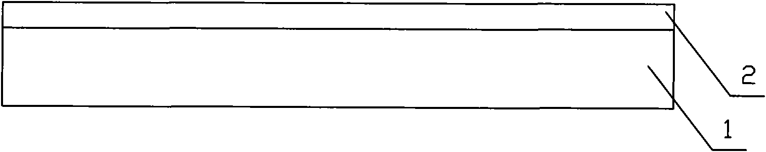
[0045] Such as figure 1 and Figure 7 As shown: (1) First, on the lower substrate 1 of the field emission display after being ultrasonically cleaned with acetone, the grid electrode layer 2 comprising a plurality of parallel strip grid electrodes is directly printed by screen printing, and the grid electrode layer 2 is directly printed at 100 ℃, under normal pressure, drying for 20 minutes, and then at 570 ℃, under normal pressure, sintering for 20 minutes; the material of the gate electrode layer 2 is silver paste.
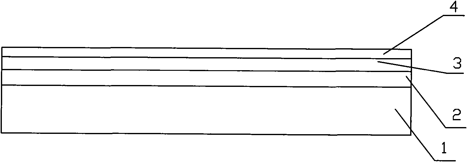
[0046] Such as figure 2 As shown: (2) Print the entire surface of the water-soluble insulating medium layer 3 on the gate electrode layer 2, and dry the water-soluble insulating medium layer 3 at 130°C under normal pressure for 10 minutes, then at 580°C, Under normal pressure, sinter for 20 minutes.
[0047] (3) Then print the entire cathode electrode layer 4 on the water-soluble insulating medium layer 3 after sintering, and then dry it for 30 minutes at 80°...
Embodiment 2
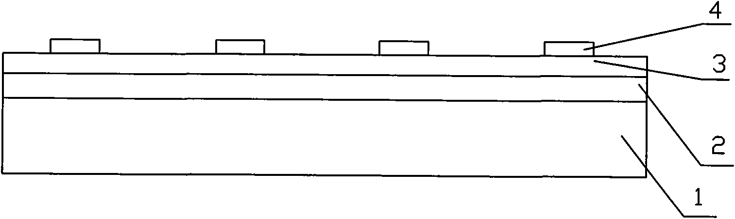
[0064] Such as figure 1 and Figure 7 Shown: (1) Print the entire gate electrode layer 2 on the lower substrate 1 of the field emission display after being ultrasonically cleaned with acetone, and then dry it for 30 minutes at 100° C. under normal pressure. Using the film graphic model of the gate electrode layer as a mask, the entire gate electrode layer 2 is exposed and developed by photolithography, so that the entire gate electrode layer 2 forms a grid consisting of multiple parallel strip gate electrodes. Gate electrode layer 2 ; then, the gate electrode layer 2 after photolithography was sintered at 570° C. under normal pressure for 20 minutes. The exposure energy is 800mJ, and the developing solution is 0.3% sodium carbonate solution. The material of the gate electrode layer 2 is photosensitive silver paste.
[0065] Such as figure 2 As shown: (2) Print the first layer of the entire surface of the water-soluble insulating dielectric layer 3 on the sintered gate ele...
PUM
 Abstract
Description
Claims
Application Information
 - R&D
- Intellectual Property
- Life Sciences
- Materials
- Tech Scout
- Unparalleled Data Quality
- Higher Quality Content
- 60% Fewer Hallucinations
Browse by: Latest US Patents, China's latest patents, Technical Efficacy Thesaurus, Application Domain, Technology Topic, Popular Technical Reports.
© 2025 PatSnap. All rights reserved.Legal|Privacy policy|Modern Slavery Act Transparency Statement|Sitemap|About US| Contact US: help@patsnap.com