
Novel process for all-component high-added-value clean utilization of waste circuit boards

A waste circuit board and full-component technology, which is applied in the field of high-value clean utilization of waste circuit boards with full components, can solve the problem of inability to disassemble electronic components, circuit boards, recovery of metals such as lead and tin, and production and processing costs. High problems, to achieve the effect of being conducive to centralized treatment, improving copper purity, and improving recovery rate

Inactive Publication Date: 2009-11-04
JIANGSU TEACHERS UNIV OF TECH +1
View PDF4 Cites 19 Cited by
  • Summary
  • Abstract
  • Description
  • Claims
  • Application Information

AI Technical Summary

Problems solved by technology

This method needs to feed liquid nitrogen continuously in the whole pulverization process, so the cost of recovery is high
[0009] In addition to the above technologies, there are some immature treatment methods such as microwave treatment technology and biological treatment, which are still in the exploratory stage.
In short, the existing recycling technologies for waste circuit boards either have a low resource recovery rate, have a great impact on the environment, or have high production and processing costs. dismantling, lead, tin and other metals cannot be recovered, so the above methods cannot meet the requirements of the market

Method used


Image

  • Novel process for all-component high-added-value clean utilization of waste circuit boards
  • Novel process for all-component high-added-value clean utilization of waste circuit boards
  • Novel process for all-component high-added-value clean utilization of waste circuit boards

Examples


Embodiment Construction

[0042] The specific embodiments of the present invention will be further described in detail below in conjunction with the accompanying drawings.

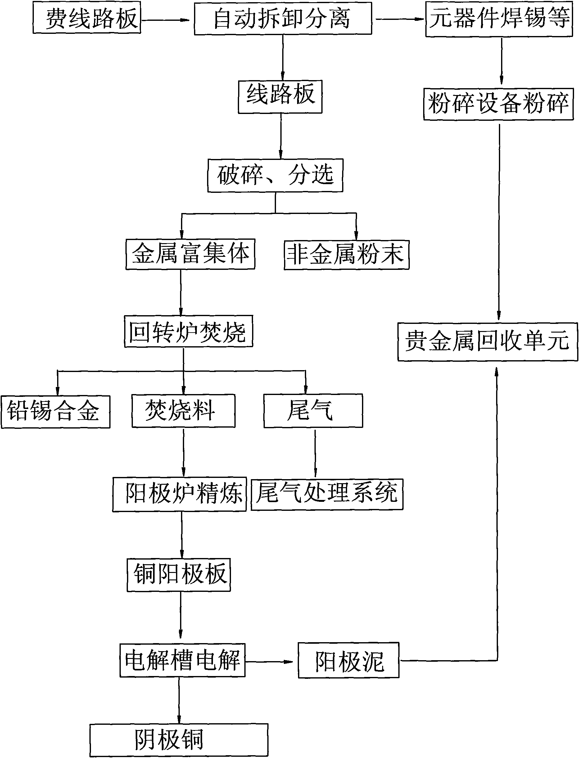
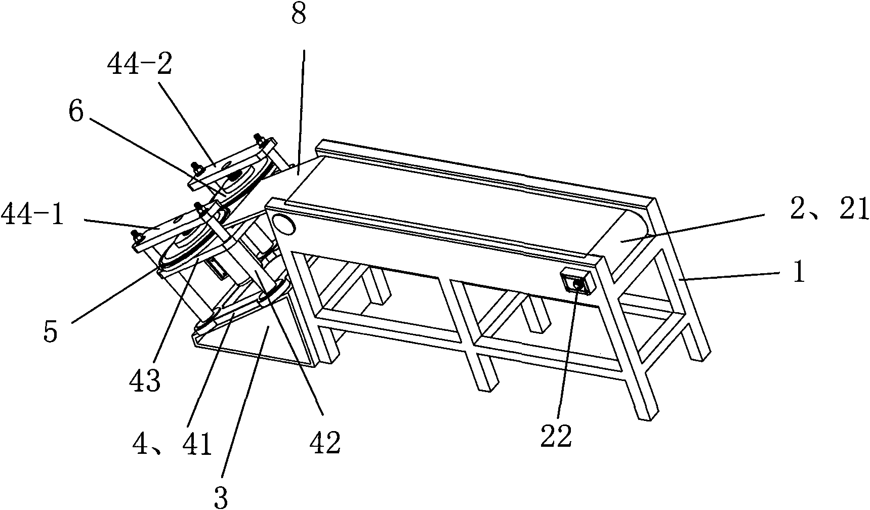
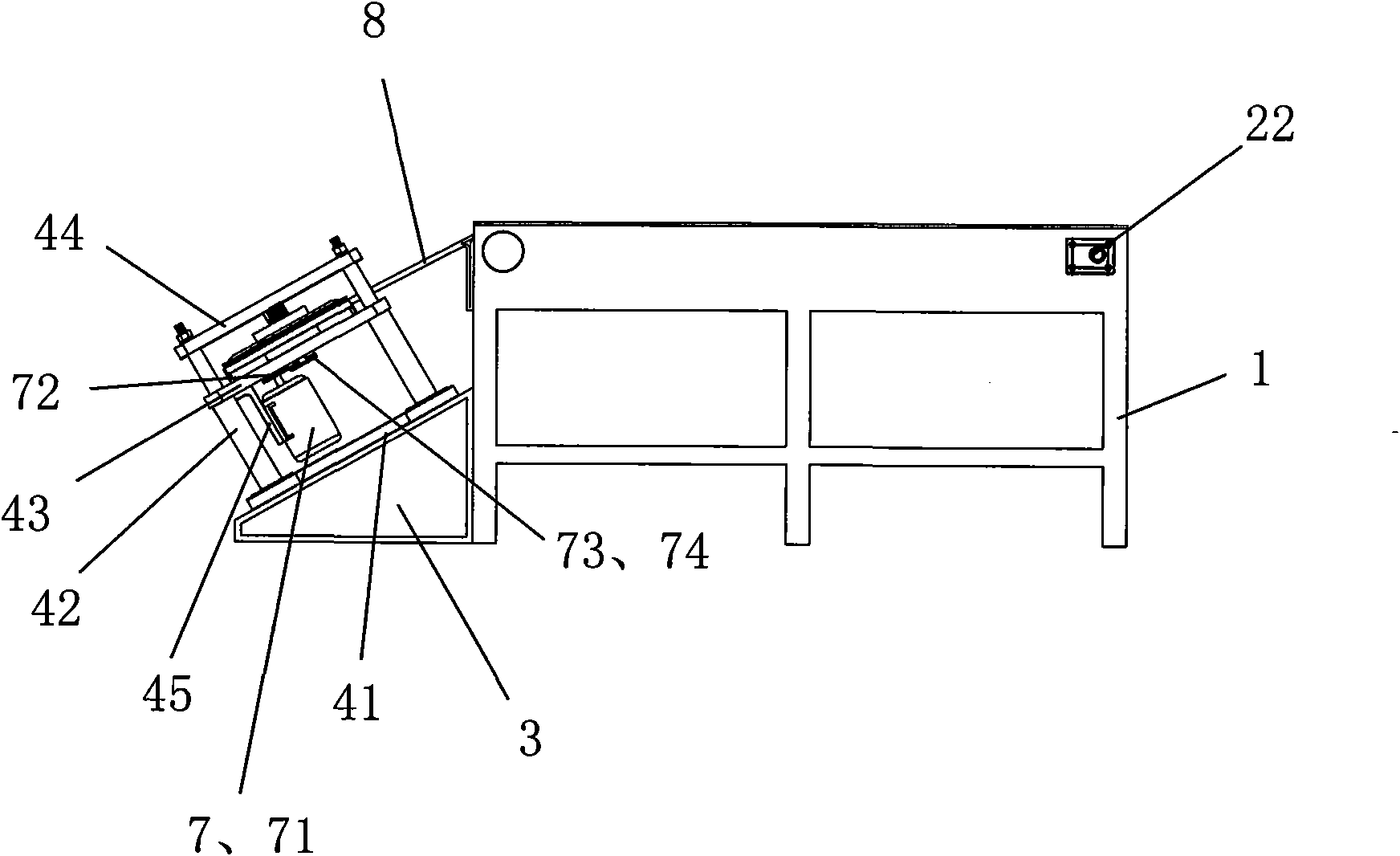
[0043] Such as figure 1 As shown: the new high-value cleaning and utilization process of waste circuit boards of the present invention includes the following steps: (a) the waste circuit boards with components are separated from the circuit boards by an automatic dismantling and sorting device ;Using the shearing pulverizer to crush components as raw materials for precious metal deep processing units, which is conducive to the centralized treatment of gold, silver, platinum, palladium and other precious metals on components, and can also reduce components from being broken with waste circuit boards, The loss of precious metals caused by crushing and sorting; (b) using a pneumatic crusher to crush the circuit board, the crushed powder is screened through 2mm, and the powder below 2mm is separated by sorting to obtain rough copper po...


PUM


Abstract

The invention relates to a novel process for all-component high-added-value clean utilization of waste circuit boards, which comprises the steps: a) automatically disassembling and separating the waste circuit boards, crushing separated electronic components and then taking the crushed electronic components as a unit raw material for deep processing of precious metals; b) crushing the separated circuit boards by a crushing machine, and then obtaining a metal concentrate and nonmetal powder through air separation; c) sending the metal concentrate into a rotary incinerator for incineration, removing resin organic substances, and separating low melting point metals such as lead, tin and the like to form alloy recovery; d) sending an incineration material into an anode furnace, and casting melt subjected to oxidation reduction refining to obtain a copper anode plate; e) electrolyzing the copper anode plate to obtain a copper cathode plate and anode mud, and taking the anode mud as a unit raw material for the deep processing of the precious metals; and f) treating the unit raw materials for the deep processing of the precious metals to obtain the precious metals such as gold, silver and the like. The process mainly adopts a combined flow of automatic disassembly classification, a pyrogenic process and a wet process to treat the waste circuit boards; and the process has the advantages of high recovery rate, small energy consumption and less pollution on the environment.

Description

technical field [0001] The invention belongs to the field of electronic waste recycling, in particular to a process method for high-value clean utilization of all components of waste circuit boards. Background technique [0002] With the rapid development of electronic information technology, the use of electronic products is expanding, and the speed of replacement is accelerating. Electronic waste (WEEE, commonly known as electronic waste, mainly refers to discarded household appliances, communication tools, battery products and the production process of these products. The production speed and volume of all kinds of scrap products, scraps and sludge wastes produced in the electronic waste have become the fastest growing waste in the urban waste. [0003] However, e-waste has dual attributes: resource and pollution. Resource means that e-waste contains a lot of recyclable non-ferrous metals, ferrous metals, glass, plastics and other substances. According to data, e-waste T...

Claims


Application Information

Patent Timeline
IPC IPC(8): B09B3/00
CPCY02W30/20Y02W30/82
Inventor 张锁荣周全法朱炳龙王怀栋
Owner JIANGSU TEACHERS UNIV OF TECH
Learn More